
XCV600E-6BG432C
| Part Description |
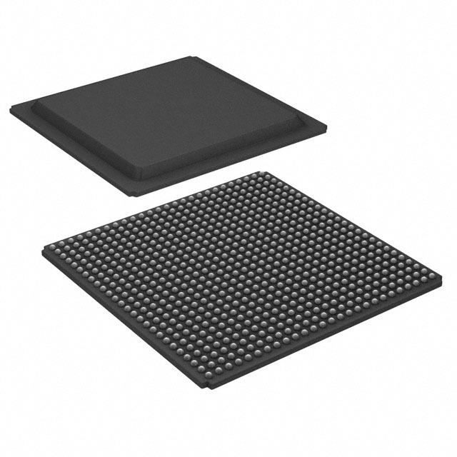
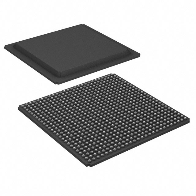
Virtex®-E Field Programmable Gate Array (FPGA) IC 316 294912 15552 432-LBGA Exposed Pad, Metal |
|---|---|
| Quantity | 511 Available (as of October 8, 2026) |

| Product Category | Field Programmable Gate Array (FPGA) |
|---|---|
| Manufacturer | AMD |
| Manufacturing Status | Obsolete |
| Manufacturer Standard Lead Time | Contact Us |
| Datasheet |
Specifications & Environmental
| Device Package | 432-MBGA (40x40) | Grade | Commercial | Operating Temperature | 0°C – 85°C | ||
|---|---|---|---|---|---|---|---|
| Package / Case | 432-LBGA Exposed Pad, Metal | Number of I/O | 316 | Voltage | 1.71 V - 1.89 V | ||
| Mounting Method | Surface Mount | RoHS Compliance | RoHS non-compliant | REACH Compliance | REACH Unaffected | ||
| Moisture Sensitivity Level | 3 (168 Hours) | Number of LABs/CLBs | 3456 | Number of Logic Elements/Cells | 15552 | ||
| Number of Gates | 985882 | ECCN | 3A991D | HTS Code | 8542.39.0001 | ||
| Qualification | N/A | Total RAM Bits | 294912 |
Overview of XCV600E-6BG432C – Virtex®-E Field Programmable Gate Array, 432-LBGA
The XCV600E-6BG432C is a Virtex®-E series Field Programmable Gate Array (FPGA) in a 432-ball LBGA exposed-pad metal package designed for commercial-grade, surface-mount applications. It delivers a high-density, reprogrammable logic fabric with a 1.8 V-class core (specified supply 1.71 V to 1.89 V) and is intended for designs requiring substantial I/O counts and embedded memory.
Typical use cases include high-performance interface controllers, memory subsystem logic, and complex custom digital functions where integration, reconfigurability and on-chip resources are important for reducing overall system complexity.
Key Features
- Logic Capacity Provides 15,552 logic elements (logic cells) and approximately 985,882 equivalent gates for implementing complex combinational and sequential logic.
- Embedded Memory Approximately 0.295 Mbits of on-chip RAM (294,912 total RAM bits) to support buffering, FIFOs and small on-chip data stores.
- I/O Density & Flexibility 316 user I/O pins enable high pin-count designs and flexible interface routing for mixed-signal and high-speed I/O requirements.
- Clock Management Series-level clock management features include multiple fully digital delay-locked loops, enabling deterministic clocking and DDR-friendly timing architectures.
- High-Speed Interface Support Virtex®-E SelectI/O+ technology (series feature) provides broad interface standard support and differential signaling capabilities for high-bandwidth applications.
- Package & Mounting 432-LBGA exposed pad, metal package (supplier package 432-MBGA, 40×40) delivered in a surface-mount form factor for compact board-level integration.
- Power & Temperature Core supply specified 1.71 V to 1.89 V and commercial operating temperature range 0 °C to 85 °C.
- Compliance RoHS compliant and 100% factory tested as part of the Virtex®-E family production specifications.
Typical Applications
- High-performance interface bridging Use for PCI-compliant and other bus-interface logic where flexible I/O and reprogrammability help implement complex protocol bridges and timing adaptations.
- Memory controller and buffering Leverage on-chip RAM and SelectRAM+ memory hierarchy features for interfacing to ZBT SRAMs and DDR SDRAMs and for high-bandwidth buffering.
- High-speed serial and differential signaling Implement LVDS/LVPECL/BLVDS and other differential interfaces supported by the Virtex®-E series for low-jitter clocking and high-rate data paths.
- Reconfigurable system logic Ideal for in-system programmable designs requiring field updates, prototyping, and deployment of custom digital accelerators or control logic.
Unique Advantages
- Significant on-chip logic and gates: 15,552 logic elements and nearly one million equivalent gates enable dense implementation of custom logic with fewer external components.
- Integrated memory resources: Approximately 0.295 Mbits of embedded RAM reduces dependence on external memory for small buffers and control structures.
- High I/O count with flexible standards: 316 I/Os and SelectI/O+ series capabilities support a wide range of interface standards and differential signaling for system-level connectivity.
- Deterministic clocking: Multiple digital DLLs (series feature) provide precise clock management for DDR and high-speed synchronous designs.
- Compact, manufacturable package: 432-LBGA exposed-pad metal package in a 40×40 supplier footprint simplifies board placement and thermal conduction for surface-mount assembly.
- Commercial-grade, RoHS compliant: Designed for commercial temperature operation (0 °C to 85 °C) and compliant with RoHS requirements for environmental compatibility.
Why Choose XCV600E-6BG432C?
The XCV600E-6BG432C combines a high logic element count, substantial gate-equivalent capacity and on-chip memory with a large, flexible I/O complement in a compact LBGA package—making it well suited for designers building high-performance, reconfigurable digital systems. Its 1.8 V-class core and series-level features for high-speed interfaces and clock management support demanding timing and bandwidth requirements while enabling in-system programmability.
This device is suited for engineering teams and procurement seeking a commercially graded FPGA for communications, memory interface, prototyping, or custom logic accelerator roles where integration, reprogrammability and proven family-level capabilities are key selection criteria.
Request a quote or submit a pricing and availability inquiry to begin specifying XCV600E-6BG432C for your next design.




















Date Founded: 1969
Headquarters: Santa Clara, California, USA
Employees: 25,000+
Revenue: $22.68 Billion
Certifications and Memberships: ISO9001:2015, RoHS, REACH











