
XCV600E-8FG676C
| Part Description |
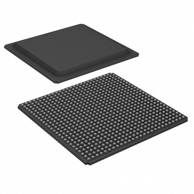
Virtex®-E Field Programmable Gate Array (FPGA) IC 444 294912 15552 676-BGA |
|---|---|
| Quantity | 1,468 Available (as of June 15, 2026) |
| Product Category | Field Programmable Gate Array (FPGA) |
|---|---|
| Manufacturer | AMD |
| Manufacturing Status | Obsolete |
| Manufacturer Standard Lead Time | Contact Us |
| Datasheet |
Specifications & Environmental
| Device Package | 676-FBGA (27x27) | Grade | Commercial | Operating Temperature | 0°C – 85°C | ||
|---|---|---|---|---|---|---|---|
| Package / Case | 676-BGA | Number of I/O | 444 | Voltage | 1.71 V - 1.89 V | ||
| Mounting Method | Surface Mount | RoHS Compliance | RoHS non-compliant | REACH Compliance | REACH Unaffected | ||
| Moisture Sensitivity Level | 3 (168 Hours) | Number of LABs/CLBs | 3456 | Number of Logic Elements/Cells | 15552 | ||
| Number of Gates | 985882 | ECCN | 3A991D | HTS Code | 8542.39.0001 | ||
| Qualification | N/A | Total RAM Bits | 294912 |
Overview of XCV600E-8FG676C – Virtex®-E 1.8 V FPGA, 676-BGA
The XCV600E-8FG676C is a Virtex®-E field programmable gate array (FPGA) from AMD in a 676-ball BGA package. It delivers a balance of logic capacity, on-chip memory and high-density I/O for demanding commercial embedded and communications designs. This device is targeted at applications that require substantial programmable logic (15,552 logic elements), extensive I/O (444 pins), and on-chip embedded memory (approximately 0.295 Mbits).
Key Features
- Core Logic — 15,552 logic elements and approximately 985,882 equivalent gates provide substantial programmable fabric for complex logic and control functions.
- Embedded Memory — Approximately 0.295 Mbits (294,912 bits) of on-chip RAM suitable for buffering, FIFOs and local data storage.
- I/O and Interfaces — 444 user I/Os available in the 676-BGA package for wide connectivity. Virtex‑E family SelectI/O+ technology supports many high‑performance interface standards and differential signalling options.
- Clocking and Timing — Family-level clock-management features include multiple digital delay‑locked loops (DLLs) and support for DDR and high-speed LVDS/LVPECL clocking as described in the Virtex‑E specification.
- Package and Mounting — 676-FBGA (27×27) surface-mount package (676-BGA) for high-density board designs and reliable solder attachment.
- Power and Supply — Internal core voltage supply specified at 1.71 V to 1.89 V (nominal 1.8 V) to match 1.8 V FPGA family power domains.
- Operating Range — Commercial grade device rated for 0 °C to 85 °C ambient operation.
- Configuration and Ecosystem (Family Capabilities) — SRAM-based in-system reprogrammability and family-level support for high-speed memory interfaces and synthesis tools as specified in the Virtex‑E documentation.
- Regulatory — RoHS compliant.
Typical Applications
- Telecommunications and Networking — High-density I/O and family support for differential and DDR interfaces make the device suitable for protocol bridging, packet processing, and front-end interface logic.
- High-Speed Data Acquisition — On-chip RAM and rich I/O coverage support buffering and aggregation of multiple high-rate data streams.
- Embedded Control and Signal Processing — Logic capacity and internal memory enable custom datapaths, finite-state machines, and preprocessing for higher-level processors.
- Memory Interface Logic — Family features target high-performance external memory interfaces and timing-critical glue logic between memory and system components.
Unique Advantages
- Substantial Logic Density: 15,552 logic elements and nearly one million equivalent gates provide the headroom for complex designs without immediate need for external ASICs.
- Comprehensive I/O Resources: 444 I/Os in a compact 676-BGA allow broad peripheral and high-speed interface support while minimizing board area.
- On-Board Memory for Low-Latency Tasks: Approximately 0.295 Mbits of embedded RAM reduces dependency on external memory for buffering and real‑time processing.
- 1.8 V Core with Standard Commercial Range: Specified 1.71–1.89 V core supply and 0 °C–85 °C operating range fit mainstream commercial applications and system power architectures.
- SRAM-Based Reprogrammability: In-system configuration enables iterative development, field updates and design flexibility during product lifecycles.
Why Choose XCV600E-8FG676C?
The XCV600E-8FG676C brings a mature Virtex‑E FPGA architecture into compact, surface-mount packaging that balances logic capacity, embedded RAM and wide I/O count for demanding commercial applications. Its 1.8 V core, commercial temperature rating and RoHS compliance make it appropriate for embedded systems, communications modules and data handling logic that require reprogrammability and in-field updates.
This device suits engineering teams who need scalable programmable logic with on-chip memory and extensive I/O, backed by the Virtex‑E family’s documented clocking, differential signalling and memory-interface features. It supports iterative development and long-term design flexibility through SRAM-based configuration.
Request a quote for XCV600E-8FG676C to check current availability and pricing or to submit a procurement inquiry.


Date Founded: 1969
Headquarters: Santa Clara, California, USA
Employees: 25,000+
Revenue: $22.68 Billion
Certifications and Memberships: ISO9001:2015, RoHS, REACH


