
XCV600E-7FG900I
| Part Description |
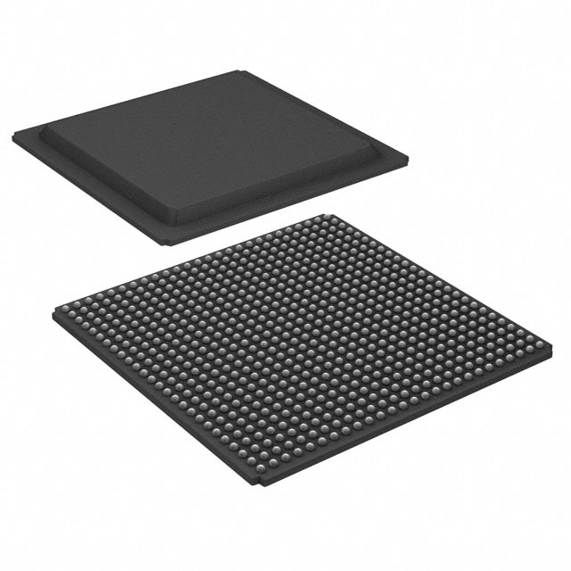
Virtex®-E Field Programmable Gate Array (FPGA) IC 512 294912 15552 900-BBGA |
|---|---|
| Quantity | 696 Available (as of October 8, 2026) |

| Product Category | Field Programmable Gate Array (FPGA) |
|---|---|
| Manufacturer | AMD |
| Manufacturing Status | Obsolete |
| Manufacturer Standard Lead Time | Contact Us |
| Datasheet |
Specifications & Environmental
| Device Package | 900-FBGA (31x31) | Grade | Industrial | Operating Temperature | -40°C – 100°C | ||
|---|---|---|---|---|---|---|---|
| Package / Case | 900-BBGA | Number of I/O | 512 | Voltage | 1.71 V - 1.89 V | ||
| Mounting Method | Surface Mount | RoHS Compliance | RoHS non-compliant | REACH Compliance | REACH Unaffected | ||
| Moisture Sensitivity Level | 3 (168 Hours) | Number of LABs/CLBs | 3456 | Number of Logic Elements/Cells | 15552 | ||
| Number of Gates | 985882 | ECCN | 3A001A7A | HTS Code | 8542.39.0001 | ||
| Qualification | N/A | Total RAM Bits | 294912 |
Overview of XCV600E-7FG900I – Virtex®-E FPGA, 512 I/O, approximately 0.295 Mbits RAM, 15,552 logic elements
The XCV600E-7FG900I is a Virtex®-E family Field Programmable Gate Array (FPGA) offered in a 900-ball BGA package for surface-mount applications. It provides a mix of programmable logic, embedded memory, and high-density I/O to support system-level functions such as high-performance interfaces, memory controllers, and custom logic acceleration.
Designed for industrial environments, this device combines a 1.71–1.89 V core supply range, broad I/O capability with 512 pins, and an operating temperature range from −40 °C to 100 °C to meet demanding embedded and systems-level applications.
Key Features
- Programmable Logic – 15,552 logic elements and approximately 985,882 gates provide the capacity to implement complex digital functions and custom processing pipelines.
- On‑chip Memory – Approximately 294,912 bits of embedded RAM (approximately 0.295 Mbits) to support FIFOs, buffers, and tightly coupled memory structures inside designs.
- I/O Capacity and SelectI/O+ Support – 512 I/O pins supporting a wide range of interface options and high aggregate bandwidth for system-level signal routing and protocol bridging.
- Differential Signalling and High‑Speed Interfaces – Series-level support for LVDS, BLVDS, and LVPECL differential signaling and up to PCI-compliant 3.3 V 32/64-bit 33/66-MHz operation as documented for the Virtex‑E family.
- Clock and Timing Resources – Family-level clock management includes multiple digitally controlled delay-locked loops (DLLs) and features for clock multiplication/division and stable DDR timing support.
- Configuration and Process – SRAM-based in-system reprogrammability with production-grade 0.18 μm process technology and 100% factory testing for consistent device delivery.
- Package and Mounting – Surface-mount 900-BBGA package (supplier device package: 900-FBGA, 31×31 mm) for compact board integration.
- Power and Temperature – Core supply range of 1.71 V to 1.89 V and industrial operating temperature range from −40 °C to 100 °C for robust field operation.
- Environmental Compliance – RoHS compliant.
Typical Applications
- High‑speed Interface Bridging – Implement PCI and other high-bandwidth interfaces using the device’s extensive I/O and differential signaling support to bridge between system buses and custom logic.
- Memory Interface and Controllers – Build controllers for external memories and buffering logic leveraging the embedded RAM and family-level support for DDR and synchronous SRAM interfaces.
- Custom Data Processing – Deploy parallel processing pipelines, protocol parsing, and hardware acceleration using the device’s abundant logic elements and on-chip memory.
- Industrial Control and Communication – Use the industrial temperature rating and extensive I/O to implement control engines, protocol converters, and field communications in industrial systems.
Unique Advantages
- Balance of Logic and Memory: The combination of 15,552 logic elements and approximately 0.295 Mbits of embedded RAM enables integrated designs that reduce external component count.
- Broad I/O Flexibility: 512 I/Os with family-level SelectI/O+ technology and differential signaling options allow straightforward integration with diverse interface standards.
- Industrial‑Grade Operation: Rated for −40 °C to 100 °C operation and RoHS compliant for deployment in industrial applications.
- Field Reprogrammability: SRAM-based in-system configuration permits design updates and iterative development without hardware changes.
- Compact, Surface‑Mount Packaging: 900-BBGA (900-FBGA 31×31) provides a high-density mounting solution for space-constrained boards.
Why Choose XCV600E-7FG900I?
The XCV600E-7FG900I positions itself as a versatile Virtex‑E FPGA option for designs requiring a strong mix of programmable logic, embedded RAM, and extensive I/O in an industrial-capable package. Its documented family features—differential signaling support, clock management resources, and in-system reprogrammability—combined with the device’s specific capacities (15,552 logic elements, ~0.295 Mbits RAM, 512 I/O) make it well suited for system interface logic, memory controllers, and custom acceleration blocks.
Choose this device when you need a proven FPGA architecture with production-tested silicon, compact BGA packaging, and the ability to adapt firmware and hardware behavior in the field while operating across a wide industrial temperature and core-voltage range.
Request a quote or submit your requirements to begin procurement and evaluation of the XCV600E-7FG900I for your next design.
























Date Founded: 1969
Headquarters: Santa Clara, California, USA
Employees: 25,000+
Revenue: $22.68 Billion
Certifications and Memberships: ISO9001:2015, RoHS, REACH











