
XCVU57P-3FSVK2892E
| Part Description |
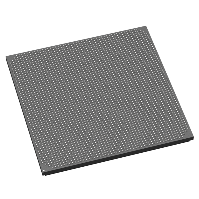
Virtex® UltraScale+™ Field Programmable Gate Array (FPGA) IC 624 74344038 2851800 2892-BBGA, FCBGA |
|---|---|
| Quantity | 198 Available (as of June 14, 2026) |
| Product Category | Field Programmable Gate Array (FPGA) |
|---|---|
| Manufacturer | AMD |
| Manufacturing Status | Last Time Buy |
| Manufacturer Standard Lead Time | 20 Weeks |
| Datasheet |
Specifications & Environmental
| Device Package | 2892-FCBGA (55x55) | Grade | Extended | Operating Temperature | 0°C – 100°C | ||
|---|---|---|---|---|---|---|---|
| Package / Case | 2892-BBGA, FCBGA | Number of I/O | 624 | Voltage | 873 mV - 927 mV | ||
| Mounting Method | Surface Mount | RoHS Compliance | ROHS3 Compliant | REACH Compliance | REACH Unknown | ||
| Moisture Sensitivity Level | 4 (72 Hours) | Number of LABs/CLBs | 162960 | Number of Logic Elements/Cells | 2851800 | ||
| Number of Gates | N/A | ECCN | 3A001A7B | HTS Code | 8542.39.0001 | ||
| Qualification | N/A | Total RAM Bits | 74344038 |
Overview of XCVU57P-3FSVK2892E – Virtex® UltraScale+™ Field Programmable Gate Array (FPGA) IC 624 74344038 2851800 2892-BBGA, FCBGA
The XCVU57P-3FSVK2892E is a Virtex® UltraScale+™ FPGA offering very high logic density and substantial on-chip memory in a 2892-ball FCBGA package. It combines a large programmable fabric with a high I/O count and a narrow core voltage range to address complex, high-capacity digital designs.
Targeted for designs that require extensive programmable logic, abundant embedded memory, and numerous I/Os, this extended-grade device supports operation across a 0 °C to 100 °C range and is RoHS compliant.
Key Features
- Programmable Logic 2,851,800 logic elements to implement large-scale, custom digital architectures.
- Embedded Memory Approximately 74.34 Mbits of on-chip RAM for local buffering, state storage, and data structures.
- I/O Capacity 624 user I/O pins to interface with multiple peripherals and high-density interconnects.
- Power Core voltage supply range of 873 mV to 927 mV for core power planning and regulator selection.
- Package & Mounting 2892-ball FCBGA (2892-FCBGA, 55×55); surface-mount package suitable for high-pin-count board designs.
- Operating Range & Grade Extended grade with an operating temperature range of 0 °C to 100 °C.
- Compliance RoHS compliant.
Unique Advantages
- High logic density: 2,851,800 logic elements enable implementation of complex, large-scale designs without immediate partitioning across multiple devices.
- Substantial on-chip memory: Approximately 74.34 Mbits of embedded RAM reduces dependency on external memory for many buffering and storage needs.
- Large I/O complement: 624 I/O pins support extensive peripheral connections and high-bandwidth interfaces.
- Compact high-pin-count package: 2892-ball FCBGA (55×55) delivers high connectivity in a single, surface-mount footprint.
- Predictable power planning: A defined core voltage window (873–927 mV) simplifies regulator selection and power sequencing.
- Extended operating range: 0 °C to 100 °C grade for applications requiring broader commercial-environment robustness.
Why Choose XCVU57P-3FSVK2892E?
The XCVU57P-3FSVK2892E delivers a balance of very high logic capacity, large embedded memory resources, and a substantial I/O count within a single 2892-FCBGA package. Its extended-grade operating range and RoHS compliance make it suitable for demanding commercial and industrial-class applications that require dense programmable logic and significant on-chip storage.
As a member of the Virtex® UltraScale+™ family, this device is positioned for designs that need scalability in logic and memory while maintaining a compact, high-pin-count board footprint.
Request a quote or submit an inquiry today to discuss pricing, availability, and how the XCVU57P-3FSVK2892E can fit your next high-capacity FPGA design.


Date Founded: 1969
Headquarters: Santa Clara, California, USA
Employees: 25,000+
Revenue: $22.68 Billion
Certifications and Memberships: ISO9001:2015, RoHS, REACH


