
MCIMX233DAG4C
| Part Description |
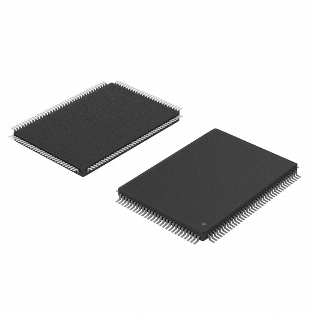
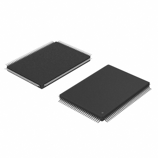
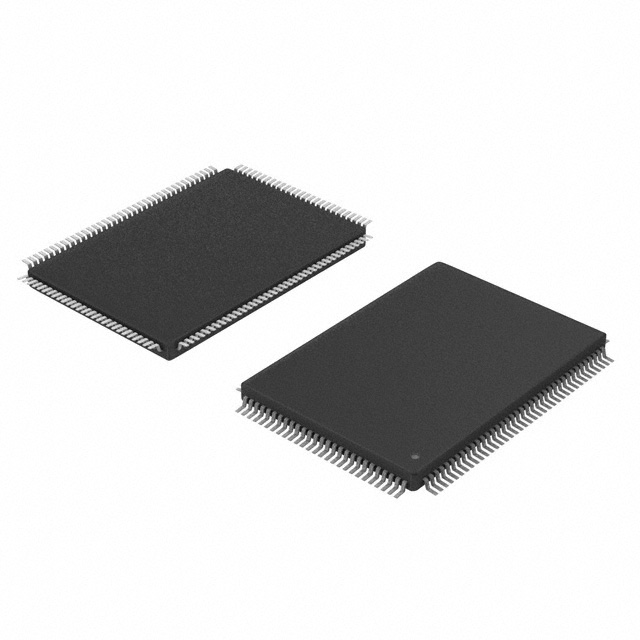
ARM926EJ-S Microprocessor IC i.MX23 1 Core, 32-Bit 454MHz 128-LQFP (14x14) |
|---|---|
| Quantity | 646 Available (as of October 8, 2026) |
| Product Category | Microprocessors |
|---|---|
| Part Series | i.MX 233 |
| Manufacturer | NXP USA Inc. |
| Manufacturing Status | Active |
| Manufacturer Standard Lead Time | 20 Weeks |
| Datasheet |
Specifications & Environmental
| Co-Processors/DSP | Data; DCP | Core Processor | ARM926EJ-S | Device Package | 128-LQFP (14x14) | ||
|---|---|---|---|---|---|---|---|
| Display & Interface Controllers | LCD, Touchscreen | ECCN | 5A992C | Graphics Acceleration | No | ||
| HTS Code | 8542.31.0001 | Moisture Sensitivity Level | 3 (168 Hours) | Mounting Method | Surface Mount | ||
| Mounting Type | Surface Mount | Number of Cores/Bus Width | 1 Core, 32-Bit | Operating Temperature | -10°C ~ 70°C (TA) | ||
| Package / Case | 128-LQFP | RAM Controllers | DRAM | REACH Compliance | REACH Unaffected | ||
| RoHS Compliance | ROHS3 Compliant | Security Features | Cryptography, Hardware ID | Speed | 454MHz | ||
| Supplier Device Package | 128-LQFP (14×14) | USB | USB 2.0 + PHY (1) | Voltage – I/O | 2.0V, 2.5V, 2.7V, 3.0V, 3.3V |
Overview of MCIMX233DAG4C – IC MPU I.MX23 454MHZ 128LQFP
The MCIMX233DAG4C is an NXP Semiconductors i.MX 233 series microprocessor featuring a single ARM926EJ-S 32‑bit core running at 454 MHz. It integrates essential system interfaces and controllers targeted at embedded applications that require a compact, surface‑mount MPU with display and USB connectivity.
Designed for embedded systems, the device pairs on‑chip interfaces (LCD and touchscreen controllers, USB 2.0 + PHY, I2C) with DRAM controller support and hardware security primitives to simplify system design and accelerate time to market.
Key Features
- Core Single ARM926EJ‑S 32‑bit core running at 454 MHz for predictable, single‑threaded embedded processing.
- Memory Support Integrated DRAM controller to interface with external memory for application and display frame buffers.
- Display and Touch On‑chip LCD and touchscreen controllers to enable local human‑machine interfaces without large external logic.
- USB Connectivity Built‑in USB 2.0 controller with integrated PHY (1) for direct peripheral and host connectivity.
- Security and Data Processing Hardware cryptography and a Hardware ID combined with a Data Co‑Processor (DCP) for secure operations and accelerated data handling.
- Peripheral Interfaces Standard embedded interfaces including I2C to connect sensors, displays, and peripheral devices.
- Package and Mounting 128‑lead LQFP package (14 × 14 mm) in a surface‑mount footprint for compact PCB designs.
- Operating Range Designed for operation from −10 °C to 70 °C to suit a range of general embedded environments.
- Environmental Compliance RoHS‑compliant manufacturing to meet common environmental requirements.
Typical Applications
- Human‑Machine Interfaces Drive LCD panels and resistive/capacitive touch inputs for compact control panels and user displays using the on‑chip display and touchscreen controllers.
- USB‑Enabled Embedded Devices Provide USB 2.0 connectivity with integrated PHY for peripherals, data transfer, and simple host/device roles.
- Secure Embedded Controllers Implement device identity and cryptographic functions using the hardware cryptography and Hardware ID features for secure boot or secure communications.
- Sensor and Peripheral Hubs Aggregate sensor data and control peripheral devices via I2C and the DRAM‑backed application space for buffering and processing.
Unique Advantages
- Integrated display and touch support: Reduces external component count by providing on‑chip LCD and touchscreen controllers for compact HMI designs.
- On‑board USB 2.0 + PHY: Simplifies system connectivity and PCB routing by including a native USB interface with physical layer.
- Security‑oriented hardware: Hardware cryptography and a Hardware ID enable device authentication and accelerated secure operations without offloading to external security chips.
- Dedicated data co‑processor: The DCP assists with data processing tasks, helping offload compute from the main CPU for improved system responsiveness.
- Compact surface‑mount package: 128‑LQFP (14 × 14 mm) provides a balance of IO density and board area efficiency for embedded product designs.
- RoHS compliant: Supports environmental requirements for modern electronics manufacturing.
Why Choose MCIMX233DAG4C?
MCIMX233DAG4C positions itself as a practical, integrated microprocessor option for embedded designs that need a reliable single‑core ARM926EJ‑S processor at 454 MHz with built‑in display, USB, and security capabilities. The combination of DRAM controller support, peripheral interfaces (I2C), and a dedicated data co‑processor helps streamline system architecture while preserving PCB area with a 128‑LQFP surface‑mount package.
This part is well suited to engineers building compact embedded systems requiring local displays, secure device identity, and USB connectivity. Backed by NXP Semiconductors, the MCIMX233DAG4C provides a focused feature set for straightforward integration into embedded hardware platforms.
Request a quote or submit a purchase inquiry today to evaluate MCIMX233DAG4C for your next embedded design.





















Date Founded: 2006
Headquarters: Eindhoven, North Brabant, Netherlands
Employees: 38,000+
Revenue: $10.53 Billion
Certifications and Memberships: ISO9001:2015, IATF16949:2016


