
MPC5200VR400
| Part Description |
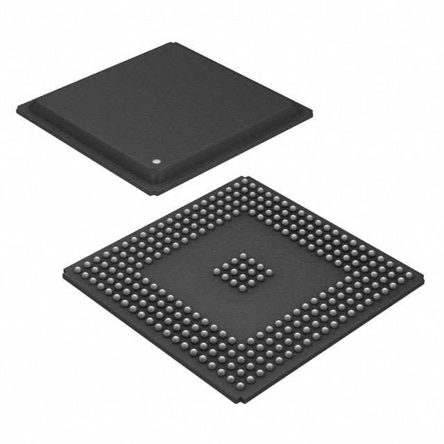
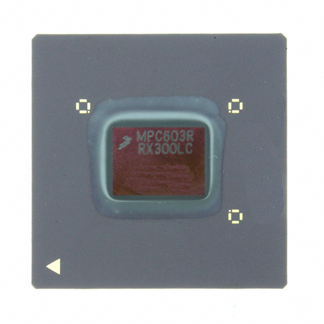
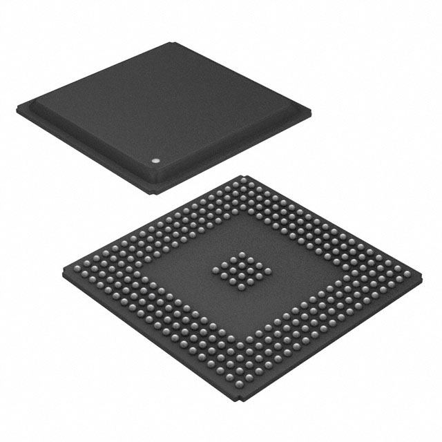
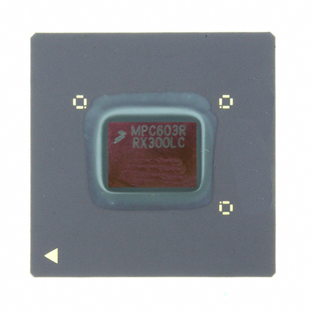
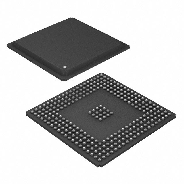
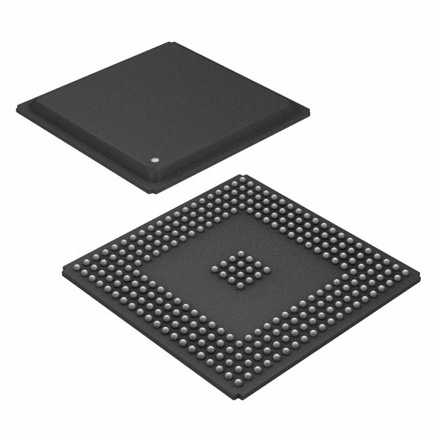
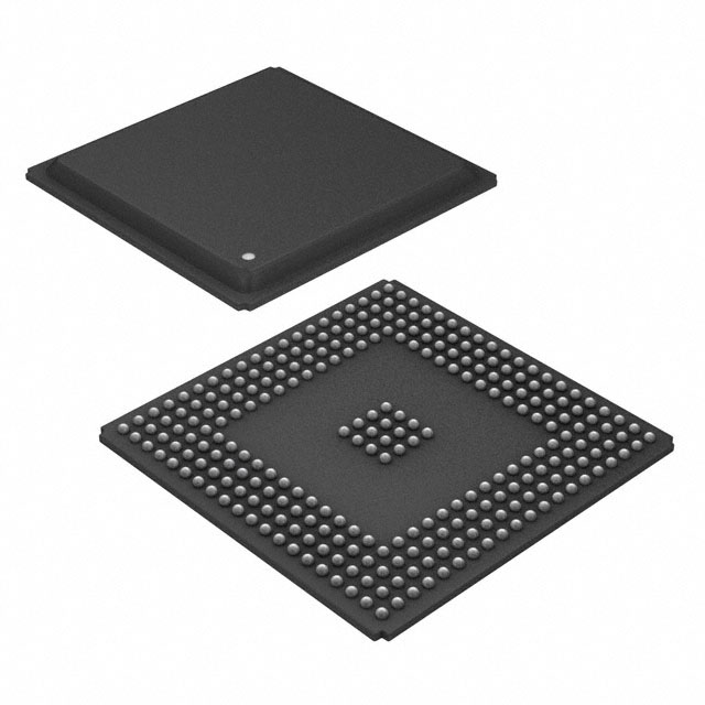
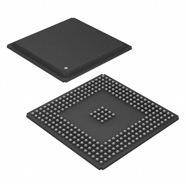
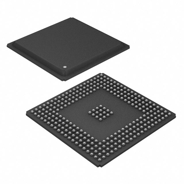
PowerPC G2_LE Microprocessor IC MPC52xx 1 Core, 32-Bit 400MHz 272-PBGA (27x27) |
|---|---|
| Quantity | 1,076 Available (as of October 7, 2026) |
| Product Category | Microprocessors |
|---|---|
| Part Series | MPC5200 |
| Manufacturer | NXP USA Inc. |
| Manufacturing Status | Not For New Designs |
| Manufacturer Standard Lead Time | 13 Weeks |
| Datasheet |
Specifications & Environmental
| Core Processor | PowerPC G2_LE | Device Package | 272-PBGA (27x27) | ECCN | 3A991A2 | ||
|---|---|---|---|---|---|---|---|
| Ethernet | 10/100Mbps (1) | Graphics Acceleration | No | HTS Code | 8542.31.0001 | ||
| Moisture Sensitivity Level | 3 (168 Hours) | Mounting Method | Surface Mount | Mounting Type | Surface Mount | ||
| Number of Cores/Bus Width | 1 Core, 32-Bit | Operating Temperature | 0°C ~ 70°C (TA) | Package / Case | 272-BBGA | ||
| RAM Controllers | DDR, SDRAM | REACH Compliance | REACH Unaffected | RoHS Compliance | ROHS3 Compliant | ||
| Speed | 400MHz | Supplier Device Package | 272-PBGA (27×27) | USB | USB 1.1 (2) | ||
| Voltage – I/O | 2.5V, 3.3V |
Overview of MPC5200VR400 – IC MPU MPC52XX 400MHZ 272BGA
The MPC5200VR400 is a single‑core, 32‑bit microprocessor based on the PowerPC G2_LE architecture, operating at 400 MHz. It integrates a breadth of peripherals and system interfaces targeted at embedded communications and systems‑integration applications, delivering a compact, high‑function embedded compute engine.
Designed for consumer‑grade embedded designs, the device combines core performance, memory flexibility and a rich I/O set to simplify system design and accelerate time to market.
Key Features
- PowerPC G2_LE core: Superscalar 32‑bit processor architecture with integrated instruction and data MMU and floating point capabilities as described in the MPC5200 series documentation.
- 400 MHz operating frequency: Processor clocked at 400 MHz for compute tasks and control functions.
- On‑chip caches and FPU: 16 KB instruction cache and 16 KB data cache plus double‑precision floating point support indicated in the MPC5200 series datasheet.
- Memory controller support: Built‑in SDRAM and DDR SDRAM controllers with initialization and refresh support and up to 132 MHz memory operation (per series documentation).
- Flexible external bus and PCI: Multifunction external bus interface and an integrated PCI controller (PCI 2.2 compatibility with 32‑bit addressing and 33/66 MHz operation noted in the series datasheet).
- Broad peripheral set: Integrated USB 1.1 (2 ports), single 10/100 Mbps Ethernet interface, ATA controller, AC97 audio interface, six programmable serial controllers (PSC), I2C, SPI, CAN and J1850 as documented in the MPC5200 series material.
- BestComm I/O subsystem: Dedicated I/O subsystem to offload routine peripheral maintenance from the core, improving deterministic behavior for communication tasks.
- Package and mounting: 272‑ball PBGA package (27 × 27 mm), surface‑mount, providing a compact footprint for board integration.
- Operating range and qualification: Consumer qualification with an operating temperature range of 0 °C to 70 °C and RoHS compliance.
Typical Applications
- Embedded communications systems: Use the integrated Ethernet, USB and serial controllers for networked appliances and communication controllers.
- Systems integration platforms: Combine external memory, PCI and multiple peripheral interfaces for compact system controllers and integration appliances.
- Consumer embedded devices: Target consumer consumer‑grade products requiring a 400 MHz PowerPC core with broad I/O and memory support.
- Storage and interface controllers: Leverage the ATA controller and extensive serial interfaces for storage gateways and interface bridging functions.
Unique Advantages
- Integrated communications peripherals: On‑chip Ethernet, USB, serial controllers and AC97 reduce external component count and simplify BOM.
- Single‑chip system integration: Memory controllers, PCI and BestComm DMA subsystem enable dense system designs with fewer external controllers.
- Memory flexibility: Support for SDRAM and DDR SDRAM with on‑chip initialization and refresh eases memory subsystem design and validation.
- Compact PBGA package: 272‑ball PBGA (27×27 mm) provides a high‑pin‑count solution in a space‑efficient form factor for board space constrained designs.
- Standards‑oriented connectivity: PCI controller (32‑bit, 33/66 MHz), USB 1.1 and 10/100 Ethernet enable interfacing to common industry interfaces and peripherals.
- Environmental compliance: RoHS compliant construction supports regulated product development and manufacturing processes.
Why Choose MPC5200VR400?
The MPC5200VR400 positions a 400 MHz PowerPC G2_LE core with an extensive peripheral set and flexible memory interfaces into a single consumer‑grade device. It is well suited to embedded designs that require a balanced combination of compute performance, communications capability and system integration.
Engineers designing compact, connected embedded systems will find the MPC5200VR400 offers a practical platform for reducing board complexity while retaining the interfaces and memory support needed for networking, storage and system controller applications—backed by product documentation from the MPC5200 family and NXP Semiconductors.
Request a quote or submit an inquiry to receive pricing and availability for MPC5200VR400 and support for your design requirements.





















Date Founded: 2006
Headquarters: Eindhoven, North Brabant, Netherlands
Employees: 38,000+
Revenue: $10.53 Billion
Certifications and Memberships: ISO9001:2015, IATF16949:2016


