
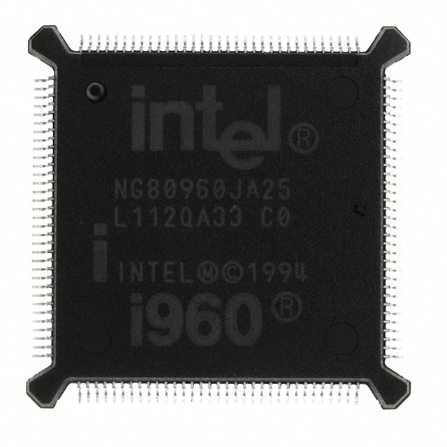
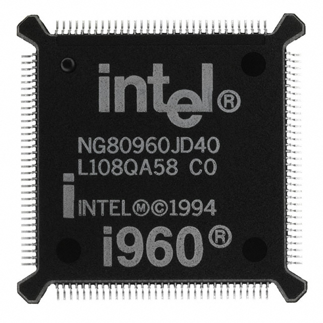
NG80960JA3V25
| Part Description |
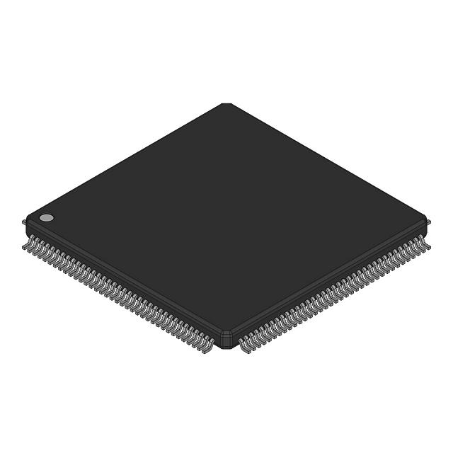
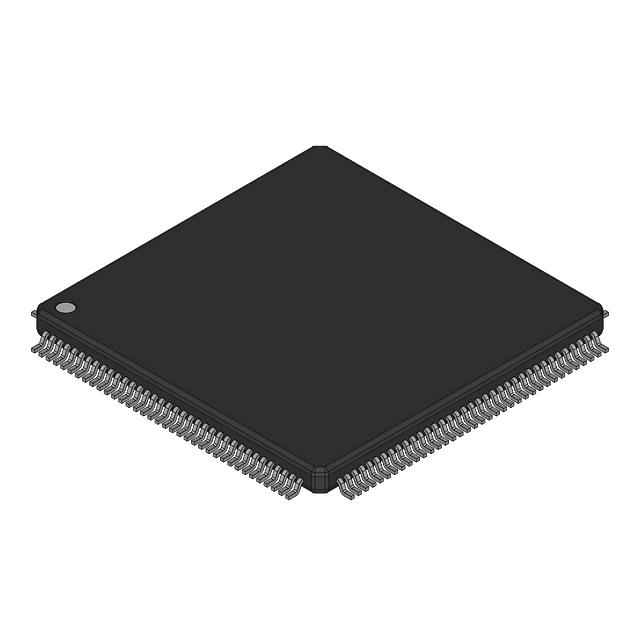
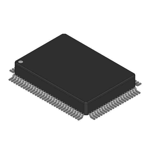
i960 Microprocessor IC i960 1 Core, 32-Bit 25MHz 132-QFP |
|---|---|
| Quantity | 488 Available (as of October 8, 2026) |
| Product Category | Microprocessors |
|---|---|
| Part Series | i960 Jx |
| Manufacturer | Intel |
| Manufacturing Status | Obsolete |
| Manufacturer Standard Lead Time | Contact Us |
| Datasheet |
Specifications & Environmental
| Core Processor | i960 | Device Package | 132-QFP | ECCN | 3A991A2 | ||
|---|---|---|---|---|---|---|---|
| Grade | Commercial | Graphics Acceleration | No | HTS Code | 8542.31.0001 | ||
| Moisture Sensitivity Level | 4 (72 Hours) | Mounting Method | Surface Mount | Mounting Type | Surface Mount | ||
| Number of Cores/Bus Width | 1 Core, 32-Bit | Operating Temperature | 0°C ~ 100°C (TC) | Package / Case | 132-QFP | ||
| REACH Compliance | REACH Unknown | RoHS Compliance | RoHS non-compliant | Speed | 25MHz | ||
| Supplier Device Package | 132-QFP | Voltage – I/O | 3.3V |
Overview of NG80960JA3V25 – IC MPU I960 25MHz 132QFP
The NG80960JA3V25 is a 32-bit embedded microprocessor based on the Intel i960 core family. This single-core device operates with a 25 MHz core clock and is supplied in a 132-lead plastic quad flat package for surface-mount assembly.
Designed for embedded applications, the device combines a compact package, on-chip memory and cache, and a 3.3 V I/O interface to support mid-range control, timing, and system integration tasks in commercial-grade environments.
Key Features
- Core Single i960 core with a 32-bit architecture and a 25 MHz core clock, delivering one instruction per clock execution as specified for the i960 Jx family.
- Memory and Cache On-chip resources include a 2 KB instruction cache and a 1 KB direct-mapped data cache for the JA variant, plus 1 KB on-chip data RAM for critical variable storage with single-cycle access.
- Buses and Interfaces High-bandwidth burst bus with 32-bit multiplexed address/data, and selectable external bus widths of 8-, 16-, or 32-bits to match system memory and peripheral configurations.
- Timers and Interrupts Two on-chip timers with independent 32-bit counting and programmable clock prescaling; a high-speed interrupt controller with programmable priorities and maskable pins.
- Power and I/O 3.3 V supply voltage with 5 V tolerant inputs and TTL-compatible outputs; includes a halt mode for low power operation.
- System and Test On-chip stack frame cache with automatic allocation on call/return and support for JTAG (IEEE 1149.1) boundary-scan for in-circuit testability.
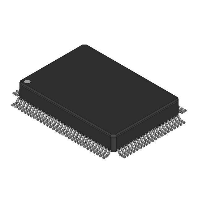
- Package and Mounting 132-lead Plastic Quad Flat Pack (132-QFP) in a surface-mount format suitable for compact embedded PCBs.
- Operating Range Commercial operating temperature range from 0 °C to 100 °C.
- Compliance RoHS compliant.
Typical Applications
- Embedded control Real-time control tasks in industrial and commercial equipment where a deterministic 32-bit core and on-chip timers are required.
- Communication and networking modules Packet handling and protocol processing that benefit from the device’s burst bus and selectable external bus widths.
- Instrumentation and measurement Local control and data collection using on-chip RAM for critical variables and single-cycle access for predictable performance.
- System controllers Board-level controller roles that leverage on-chip caches, stack frame cache, and interrupt prioritization to streamline firmware design.
Unique Advantages
- Deterministic execution: One-instruction-per-clock execution characteristic of the i960 architecture supports predictable instruction timing for real-time code.
- Integrated memory resources: Instruction and data caches plus on-chip RAM reduce dependency on external memory for performance-critical code and variables.
- Flexible system interfacing: Selectable 8/16/32-bit bus widths and a 32-bit multiplexed address/data bus simplify integration with a range of external memory and peripherals.
- 3.3 V I/O with 5 V tolerance: Native 3.3 V operation with 5 V tolerant inputs and TTL-compatible outputs eases interfacing with legacy logic levels while maintaining modern supply voltage.
- Built-in testability and low-power option: JTAG (IEEE 1149.1) boundary-scan support and a halt mode for reduced power consumption improve board-level validation and system power management.
- Code compatibility within the i960 Jx family: Series-level code compatibility supports migration and reuse of firmware across compatible i960 Jx devices.
Why Choose NG80960JA3V25?
The NG80960JA3V25 positions itself as a compact, commercially graded 32-bit microprocessor suitable for embedded designs that need deterministic execution, integrated caches, and modest on-chip RAM. Its 3.3 V I/O, 5 V tolerant inputs, and flexible bus options make it adaptable to a variety of board-level architectures.
This part is well suited to engineers seeking a code-compatible member of the i960 Jx family with proven system features—on-chip timers, interrupt prioritization, and boundary-scan—that simplify firmware and hardware validation while supporting reliable, mid-range embedded applications.
Request a quote or submit an inquiry to receive pricing and availability for NG80960JA3V25.




















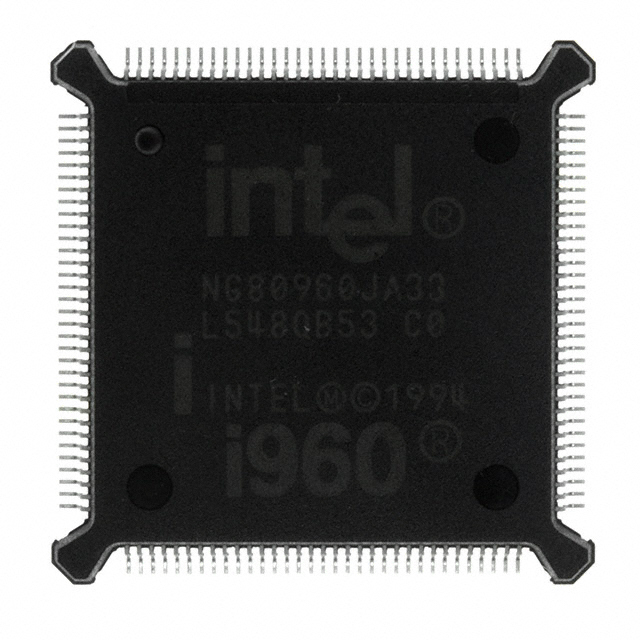
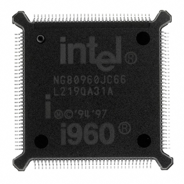
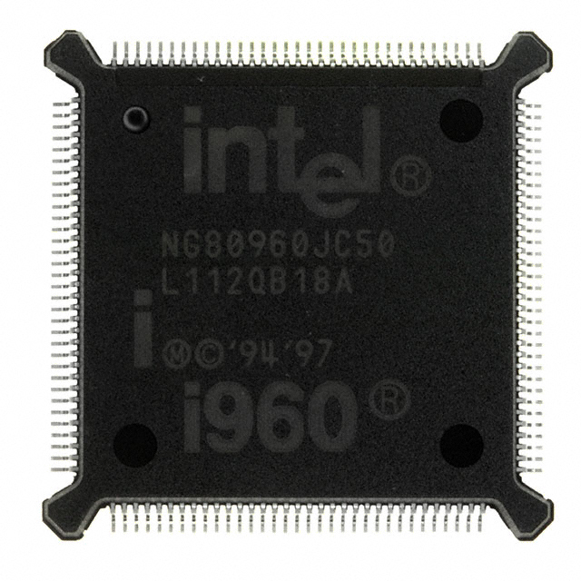

Date Founded: 1968
Headquarters: Santa Clara, California, USA
Employees: 130,000+
Revenue: $54.23 Billion
Certifications and Memberships: ISO9001:2015, ISO14001:2015, ISO17025:2017, ISO27001:2022, ISO45001:2018, ISO50001:2018


