
10AX016E3F29E2LG
| Part Description |
Arria 10 GX Field Programmable Gate Array (FPGA) IC 288 10086400 160000 780-BBGA, FCBGA |
|---|---|
| Quantity | 325 Available (as of June 15, 2026) |

| Product Category | Field Programmable Gate Array (FPGA) |
|---|---|
| Manufacturer | Intel |
| Manufacturing Status | Active |
| Manufacturer Standard Lead Time | 12 Weeks |
| Datasheet |
Specifications & Environmental
| Device Package | 780-FBGA (29x29) | Grade | Extended | Operating Temperature | 0°C – 100°C | ||
|---|---|---|---|---|---|---|---|
| Package / Case | 780-BBGA, FCBGA | Number of I/O | 288 | Voltage | 870 mV - 980 mV | ||
| Mounting Method | Surface Mount | RoHS Compliance | RoHS Compliant | REACH Compliance | REACH Unaffected | ||
| Moisture Sensitivity Level | 3 (168 Hours) | Number of LABs/CLBs | 61510 | Number of Logic Elements/Cells | 160000 | ||
| Number of Gates | N/A | ECCN | 5A002A1 | HTS Code | 8542.39.0001 | ||
| Qualification | N/A | Total RAM Bits | 10086400 |
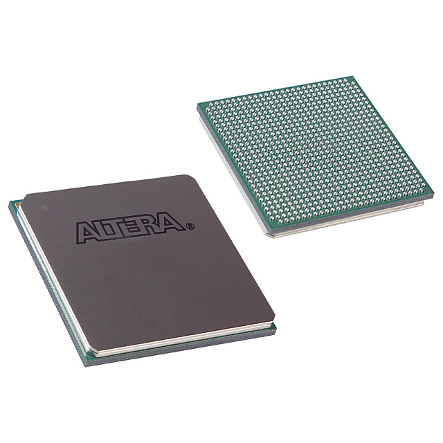
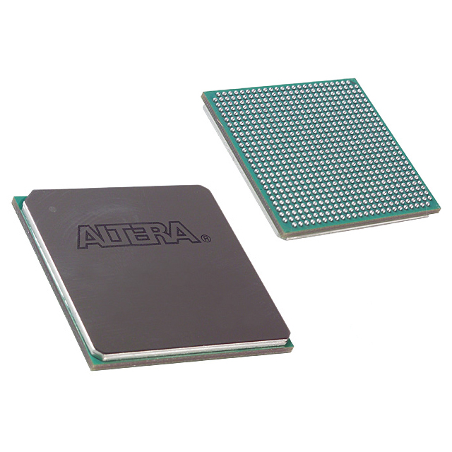
Overview of 10AX016E3F29E2LG – Arria 10 GX Field Programmable Gate Array (FPGA) IC, 780-BBGA FCBGA
The 10AX016E3F29E2LG is an Arria 10 GX FPGA in a 780-BBGA FCBGA package, built on a 20 nm mid-range FPGA/SoC architecture. It combines a high logic element count and substantial on-chip memory with integrated DSP and transceiver features to address performance- and power-sensitive applications across communications, broadcast, computing, medical and defense markets.
This device delivers a balance of logic capacity, embedded RAM and flexible I/O in a surface-mount 780-FBGA (29×29) footprint, offering designers a compact, RoHS-compliant solution for mid-range FPGA designs.
Key Features
- Core Architecture 20 nm Arria 10 GX family architecture focused on mid-range FPGA and SoC designs, emphasizing performance and power efficiency as described in the device overview.
- Logic Capacity 160,000 logic elements suitable for complex control, signal processing and protocol implementations.
- On‑Chip Memory 10,086,400 total RAM bits provided through embedded memory blocks to support buffering, packet processing and algorithm state storage.
- I/O and Package 288 I/O pins in a surface-mount 780-BBGA (FCBGA) supplier package (780-FBGA, 29×29) for flexible board-level connectivity and dense system integration.
- DSP and Transceiver Resources Includes variable-precision DSP block capability and references to low-power serial transceivers and enhanced PCS hard IP in the device family overview, useful for high-speed signal processing and serial links.
- Power Voltage supply range of 870 mV to 980 mV to match system power-rail planning and device power domains.
- Configuration and Reliability Family-level features include dynamic and partial reconfiguration, SEU error detection and correction, and support for incremental compilation as described in the device overview.
- Temperature and Grade Extended-grade device with an operating temperature range of 0 °C to 100 °C and RoHS compliance for regulatory alignment.
Typical Applications
- Wireless Infrastructure Channel and switch cards or mobile backhaul equipment leveraging on-chip DSP and logic capacity for packet processing and protocol handling.
- Wireline Networking 40G/100G muxponders, transponders and 100G line cards using embedded RAM and transceiver features for high-throughput data paths.
- Broadcast and Media Studio switches, video processing and transport applications that require dense logic, on-chip memory and deterministic I/O.
- Computing and Storage Flash cache, server acceleration and cloud server functions that benefit from programmable logic, DSP blocks and large embedded RAM.
- Medical and Defense Systems Diagnostic imaging, radar and guidance/control subsystems using the device’s logic capacity, DSP features and configuration flexibility for specialized signal processing tasks.
Unique Advantages
- High logic density: 160,000 logic elements enable implementation of substantial custom logic, control and protocol stacks without partitioning across multiple devices.
- Substantial on‑chip memory: 10,086,400 total RAM bits reduce external memory reliance for buffering and intermediate storage.
- Compact, board‑friendly package: 780-BBGA FCBGA (29×29) offers a high-pin-count, surface-mount solution for space-constrained PCBs.
- Power-optimized 20 nm architecture: Family-level emphasis on power efficiency supports designs where thermal and power budgets are constrained.
- Flexible configuration and reliability features: Support for dynamic/partial reconfiguration and SEU detection/correction helps maintain uptime and enables field-updatable designs.
- Extended operating grade and RoHS compliance: 0 °C to 100 °C operating range and RoHS status align with common commercial and industrial deployments.
Why Choose 10AX016E3F29E2LG?
The 10AX016E3F29E2LG positions itself as a balanced mid-range FPGA choice that pairs significant logic and memory resources with family-level features such as variable-precision DSP capability, transceiver support and advanced configuration options. Its extended-grade operating range, compact 780-BBGA package and RoHS compliance make it appropriate for a wide variety of commercial and industrial applications that require programmable performance and integration.
Designers targeting communications, media, storage acceleration, medical imaging or defense systems can leverage the Arria 10 GX device family characteristics and the 10AX016E3F29E2LG’s specific capacities to scale functionality while managing board space and power requirements. The device is supported by device documentation and device-specific handbook content for system integration and validation.
Request a quote or submit an RFQ to check availability and pricing for 10AX016E3F29E2LG.


Date Founded: 1968
Headquarters: Santa Clara, California, USA
Employees: 130,000+
Revenue: $54.23 Billion
Certifications and Memberships: ISO9001:2015, ISO14001:2015, ISO17025:2017, ISO27001:2022, ISO45001:2018, ISO50001:2018


