
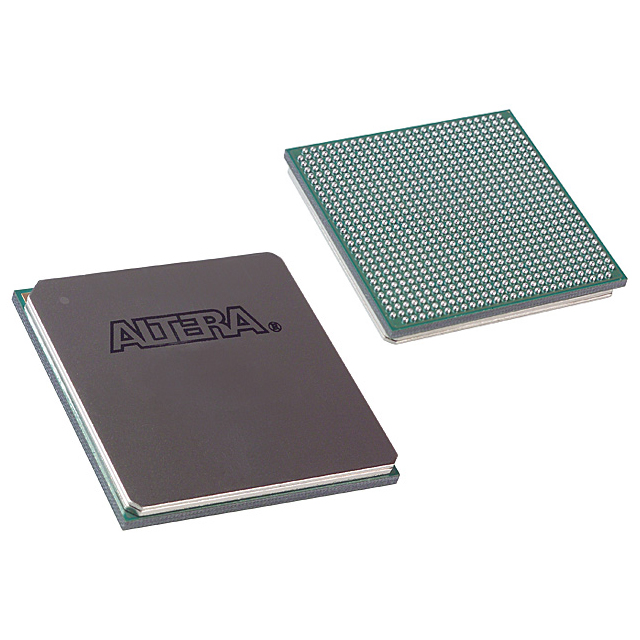
10AX016E3F29E2SG
| Part Description |
Arria 10 GX Field Programmable Gate Array (FPGA) IC 288 10086400 160000 780-BBGA, FCBGA |
|---|---|
| Quantity | 183 Available (as of June 15, 2026) |

| Product Category | Field Programmable Gate Array (FPGA) |
|---|---|
| Manufacturer | Intel |
| Manufacturing Status | Active |
| Manufacturer Standard Lead Time | 12 Weeks |
| Datasheet |
Specifications & Environmental
| Device Package | 780-FBGA (29x29) | Grade | Extended | Operating Temperature | 0°C – 100°C | ||
|---|---|---|---|---|---|---|---|
| Package / Case | 780-BBGA, FCBGA | Number of I/O | 288 | Voltage | 870 mV - 980 mV | ||
| Mounting Method | Surface Mount | RoHS Compliance | RoHS Compliant | REACH Compliance | REACH Unaffected | ||
| Moisture Sensitivity Level | 3 (168 Hours) | Number of LABs/CLBs | 61510 | Number of Logic Elements/Cells | 160000 | ||
| Number of Gates | N/A | ECCN | 5A002A1 | HTS Code | 8542.39.0001 | ||
| Qualification | N/A | Total RAM Bits | 10086400 |
Overview of 10AX016E3F29E2SG – Arria 10 GX FPGA, 780‑BBGA (288 I/O)
The 10AX016E3F29E2SG is an Intel Arria 10 GX field-programmable gate array (FPGA) in a 780-ball BGA package designed for mid-range, high-performance and power-sensitive applications. As part of the Arria 10 family, this device implements 20‑nm FPGA architecture focused on performance and power efficiency, with on-chip memory, DSP resources and flexible clocking and transceiver capabilities described for the device family.
This device targets applications across wireless, wireline, broadcast, computing, storage and defense markets where programmable logic, high I/O count and substantial on-chip memory are required along with extended operating temperature capability.
Key Features
- Logic Fabric Approximately 160,000 logic elements provide programmable logic capacity for complex mid-range designs.
- Embedded Memory About 10,086,400 total on-chip RAM bits support large buffering, packet processing and local storage needs.
- I/O Capacity 288 I/O pins allow broad external interfacing for memory, SerDes front-ends and system control signals.
- Device Family Capabilities Arria 10 devices include adaptive logic modules, variable-precision DSP blocks, clock networks and PLL clock sources per the device family overview.
- High-speed Interfaces (family) Arria 10 device documentation lists PCIe Gen1/2/3 hard IP, enhanced PCS for Interlaken and 10 Gbps Ethernet, and low-power serial transceivers as family-level features.
- Power and Supply Core supply range is specified from 870 mV to 980 mV to meet the device’s power requirements.
- Package & Mounting 780‑BBGA (FCBGA) package, supplier package noted as 780‑FBGA (29×29), optimized for surface-mount assembly.
- Operating Range & Grade Extended grade with an operating temperature range of 0 °C to 100 °C.
- Compliance RoHS compliant.
Typical Applications
- Wireless Infrastructure Channel and switch cards in remote radio heads and mobile backhaul systems where programmable logic and efficient data handling are required.
- Wireline & Networking 40G/100G muxponders, transponders and line cards benefiting from on-chip memory and high-speed interface capabilities.
- Broadcast & Professional AV Studio switches, transport and video-processing systems that need flexible I/O and significant local RAM for buffering and frame processing.
- Compute & Storage Acceleration Flash cache, server acceleration and cloud infrastructure tasks that leverage DSP blocks and reconfigurable logic for custom acceleration.
Unique Advantages
- High Logic Density: ~160,000 logic elements enable integration of complex functions and system-level consolidation on a single device.
- Substantial On‑Chip RAM: Over 10 million bits of embedded RAM reduce external memory dependence for buffering and packet handling.
- Rich I/O Count: 288 I/O pins provide flexible connectivity for external memories, high-speed links and control interfaces.
- Family-Level High-Speed IP: Arria 10 family support for PCIe Gen1/2/3 and high‑speed Ethernet/Interlaken PHYs simplifies integration of standard interfaces.
- Power-Aware Architecture: Part of a 20‑nm family designed with power-efficiency technologies to help manage thermal and power budgets.
- Extended Operating Grade: 0 °C to 100 °C operating range and surface-mount 780‑BBGA packaging suited to many board-level deployments.
Why Choose 10AX016E3F29E2SG?
The 10AX016E3F29E2SG delivers a balance of logic capacity, on‑chip memory and I/O breadth in a 20‑nm Arria 10 GX device. Its specifications make it suitable for mid-range applications that require programmable performance with attention to power efficiency and integration density.
Design teams looking to implement packet processing, interface bridging, acceleration or high-speed connectivity functions will find this device appropriate for consolidating system functions while retaining the flexibility of FPGA-based reprogrammability and the documented Arria 10 device-level capabilities such as DSP blocks, PLLs and high-speed transceiver support.
Request a quote or submit an inquiry to receive availability and pricing information for 10AX016E3F29E2SG. Our team can provide procurement details and help assess fit for your design.


Date Founded: 1968
Headquarters: Santa Clara, California, USA
Employees: 130,000+
Revenue: $54.23 Billion
Certifications and Memberships: ISO9001:2015, ISO14001:2015, ISO17025:2017, ISO27001:2022, ISO45001:2018, ISO50001:2018


