
10AX027E4F27E3SG
| Part Description |
Arria 10 GX Field Programmable Gate Array (FPGA) IC 240 17870848 270000 672-BBGA, FCBGA |
|---|---|
| Quantity | 236 Available (as of June 10, 2026) |

| Product Category | Field Programmable Gate Array (FPGA) |
|---|---|
| Manufacturer | Intel |
| Manufacturing Status | Active |
| Manufacturer Standard Lead Time | 16 Weeks |
| Datasheet |
Specifications & Environmental
| Device Package | 672-FBGA, FC (27x27) | Grade | Extended | Operating Temperature | 0°C – 100°C | ||
|---|---|---|---|---|---|---|---|
| Package / Case | 672-BBGA, FCBGA | Number of I/O | 240 | Voltage | 870 mV - 980 mV | ||
| Mounting Method | Surface Mount | RoHS Compliance | RoHS Compliant | REACH Compliance | REACH Unaffected | ||
| Moisture Sensitivity Level | 3 (168 Hours) | Number of LABs/CLBs | 101620 | Number of Logic Elements/Cells | 270000 | ||
| Number of Gates | N/A | ECCN | 5A002A1 | HTS Code | 8542.39.0001 | ||
| Qualification | N/A | Total RAM Bits | 17870848 |
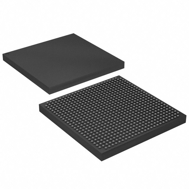
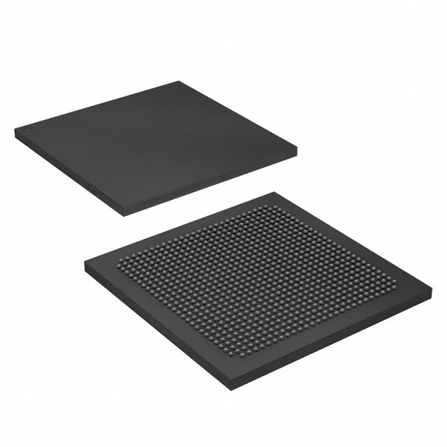
Overview of 10AX027E4F27E3SG – Arria 10 GX FPGA, 672‑BBGA FCBGA, 240 I/Os
The 10AX027E4F27E3SG is an Intel Arria 10 GX family field‑programmable gate array (FPGA) supplied in a 672‑ball BGA (FCBGA) package. It combines a high count of programmable logic with substantial on‑chip memory and flexible I/O, targeting mid‑range applications that require a balance of performance and power efficiency.
Members of the Arria 10 family are described as 20‑nm mid‑range FPGAs and SoCs suitable for markets such as wireless, wireline, broadcast, computing and storage, medical, and defense—applications where performance, power management, and integration are important design drivers.
Key Features
- Logic Capacity Contains 270,000 logic elements to implement complex digital functions and custom processing pipelines.
- On‑Chip Memory Includes 17,870,848 total RAM bits for embedded buffering, state storage, and memory‑intensive logic.
- I/O Count Provides 240 user I/O pins to support multiple external interfaces and parallel data paths.
- Package Supplied in a 672‑BBGA (FCBGA) package; supplier device package listed as 672‑FBGA, FC (27×27) for high‑density board integration.
- Voltage Supply Operates from 870 mV to 980 mV, supporting low‑voltage core operation as specified.
- Thermal and Grade Extended grade device with an operating temperature range of 0 °C to 100 °C for a variety of commercial and rugged environments.
- Family Features (Arria 10) Includes family‑level capabilities described in the Arria 10 device overview such as variable‑precision DSP blocks, embedded memory blocks, clock networks and PLLs, low‑power serial transceivers, PCIe hard IP, and support for dynamic and partial reconfiguration.
- Standards and Compliance RoHS compliant for environmental and lead‑free manufacturing requirements.
Typical Applications
- Wireless Infrastructure Channel and switch cards in remote radio heads and mobile backhaul equipment where programmable logic and DSP resources are needed.
- Wireline Communications 40G/100G muxponders, transponders and line cards that require high I/O density and on‑chip memory for packet buffering and interface logic.
- Broadcast and Pro AV Studio switches, transport and professional audio/video equipment leveraging the FPGA’s integration and processing capabilities.
- Computing and Storage Flash cache, server acceleration and cloud compute nodes that benefit from programmable acceleration and embedded memory.
- Medical and Defense Systems Diagnostic imaging and radar or guidance control subsystems where configurable logic and deterministic behavior are required.
Unique Advantages
- High logic density: 270,000 logic elements enable complex algorithms and wide datapaths without external ASICs.
- Substantial embedded memory: 17,870,848 RAM bits reduce reliance on external memory for many buffering and storage tasks.
- Flexible I/O and packaging: 240 I/Os in a 672‑BBGA FCBGA footprint supports dense board layouts and varied interface requirements.
- Low‑voltage core operation: Specified 870 mV to 980 mV supply supports designs targeting reduced core power consumption.
- Extended temperature grade: Rated for 0 °C to 100 °C operation to accommodate a wide range of commercial and rugged deployments.
- Family ecosystems and features: Leverages Arria 10 family capabilities—DSP blocks, PLLs, transceivers, PCIe hard IP and reconfiguration features—for integrated system design.
Why Choose 10AX027E4F27E3SG?
The 10AX027E4F27E3SG delivers a balance of programmable logic capacity, on‑chip memory, and I/O density in a compact 672‑BBGA package, targeting mid‑range designs that need both performance and power efficiency. As a member of the Intel Arria 10 GX family, it brings established family‑level features—DSP blocks, embedded memory, transceivers and hard IP—that support diverse markets from communications to storage and industrial imaging.
This device is suited for engineers and system designers who require a scalable, documented FPGA platform with verifiable specifications for voltage, temperature, package, and environmental compliance.
Request a quote or submit a purchase inquiry to check availability and lead times for part number 10AX027E4F27E3SG.


Date Founded: 1968
Headquarters: Santa Clara, California, USA
Employees: 130,000+
Revenue: $54.23 Billion
Certifications and Memberships: ISO9001:2015, ISO14001:2015, ISO17025:2017, ISO27001:2022, ISO45001:2018, ISO50001:2018


