
10AX115N4F45I3SGE2
| Part Description |
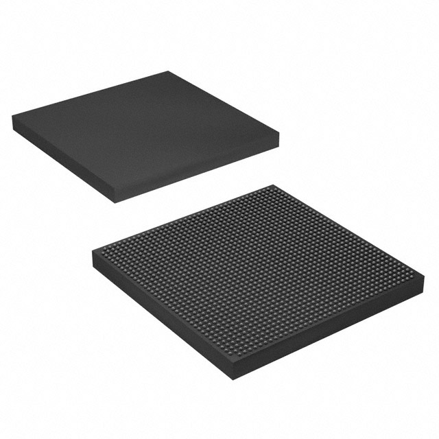
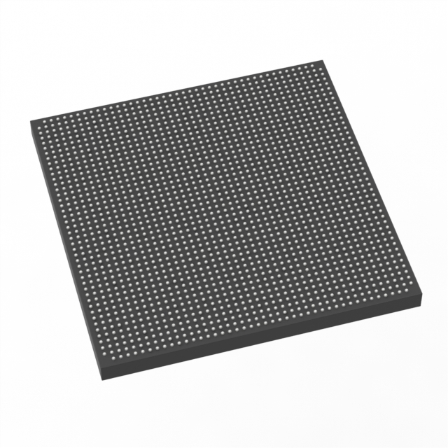
Arria 10 GX Field Programmable Gate Array (FPGA) IC 768 68857856 1150000 1932-BBGA, FCBGA |
|---|---|
| Quantity | 404 Available (as of June 18, 2026) |

| Product Category | Field Programmable Gate Array (FPGA) |
|---|---|
| Manufacturer | Intel |
| Manufacturing Status | Discontinued |
| Manufacturer Standard Lead Time | 6 Weeks |
| Datasheet |
Specifications & Environmental
| Device Package | 1932-FCBGA (45x45) | Grade | Industrial | Operating Temperature | -40°C – 100°C | ||
|---|---|---|---|---|---|---|---|
| Package / Case | 1932-BBGA, FCBGA | Number of I/O | 768 | Voltage | 870 mV - 930 mV | ||
| Mounting Method | Surface Mount | RoHS Compliance | RoHS Compliant | REACH Compliance | REACH Unaffected | ||
| Moisture Sensitivity Level | 3 (168 Hours) | Number of LABs/CLBs | 427200 | Number of Logic Elements/Cells | 1150000 | ||
| Number of Gates | N/A | ECCN | 3A001A7A | HTS Code | 8542.39.0001 | ||
| Qualification | N/A | Total RAM Bits | 68857856 |
Overview of 10AX115N4F45I3SGE2 – Arria 10 GX FPGA, 1932-FCBGA (45×45)
The 10AX115N4F45I3SGE2 is an Intel Arria 10 GX field programmable gate array in a 1932-ball FCBGA package (45×45 mm) targeted at mid‑range, high‑performance applications. It combines large programmable logic capacity, abundant on‑chip memory, and high I/O density for designs that require significant compute and connectivity resources.
Key value propositions include high logic density, extensive embedded RAM, a wide I/O count, and industrial operating range—making this device suitable for demanding communications, video, storage, and industrial systems that benefit from a configurable hardware platform.
Key Features
- Logic Capacity Approximately 1,150,000 logic elements, enabling complex custom logic, packet processing and acceleration functions.
- Embedded Memory 68,857,856 total RAM bits on‑chip to support large buffering, lookup tables and on‑device data structures.
- I/O Density 768 device I/Os for extensive board‑level interconnect, high‑pin count interfaces, and broad peripheral support.
- Adaptive Logic & DSP Arria 10 architecture elements such as adaptive logic modules and variable‑precision DSP blocks for arithmetic-heavy or signal processing tasks.
- Transceiver and Protocol Support (Device Family) Arria 10 device family documentation references low‑power serial transceivers, hard IP for PCIe Gen1/2/3, and enhanced PCS hard IP for Interlaken and 10 Gbps Ethernet, facilitating high‑speed link implementations when used in supported device variants.
- Power and Voltage Supported core voltage supply range of 870 mV to 930 mV; family-level power management and power‑saving technologies are described in the device documentation.
- Package & Mounting 1932-ball BGA/FCBGA package (supplier device package: 1932‑FCBGA (45×45)); surface mount mounting type for standard PCB assembly.
- Industrial Temperature Range Rated for operation from −40 °C to 100 °C for industrial deployments.
- Standards & Ecosystem (Device Family) Arria 10 family documentation covers features such as clock networks, PLLs, external memory interfaces, and FPGA configuration options to support complex system integration.
Typical Applications
- Wireless Infrastructure Channel and switch cards or mobile backhaul equipment that need programmable logic and high I/O to implement baseband processing and control functions.
- Wireline & Networking 40G/100G muxponders, transponders, and line cards that require on‑chip DSP, high‑speed transceivers, and substantial buffering.
- Broadcast & Professional Video Studio switches and video transport nodes where large logic capacity and embedded memory enable real‑time video processing and routing.
- Computing & Storage Server acceleration and flash cache controllers that benefit from programmable hardware acceleration and extensive on‑device memory.
Unique Advantages
- High Logic Density: With ~1,150,000 logic elements, the device supports large, complex designs without immediate migration to larger product tiers.
- Large On‑Chip Memory: 68,857,856 total RAM bits reduce dependence on external memory for buffering and lookup functions, simplifying board design.
- Extensive I/O Count: 768 I/Os provide flexible connectivity for multi‑lane interfaces, parallel buses, and numerous peripherals.
- Industrial Operating Range: −40 °C to 100 °C rating supports deployment in temperature‑challenging environments.
- High‑Pin FCBGA Package: 1932-ball 45×45 FCBGA enables dense routing and high‑speed signal integrity for complex system integration.
- Family Ecosystem: Arria 10 family documentation and design resources cover clocking, transceivers, and IP blocks (PCIe, Ethernet, Interlaken) to accelerate development when using supported device variants.
Why Choose 10AX115N4F45I3SGE2?
This Arria 10 GX FPGA part combines substantial programmable logic, large embedded RAM, and a high I/O count in an industrial‑rated, high‑pin‑count FCBGA package. It is positioned for mid‑range systems that require configurable hardware acceleration, significant on‑chip memory, and extensive board connectivity without sacrificing thermal and voltage operating margins.
Designers building communications, broadcast, compute acceleration or industrial control systems will find this device suited for scalable, long‑lifecycle projects where performance, integration density, and documented device family features support complex implementations and iterative development.
Request a quote or submit an inquiry to receive pricing, availability, and delivery information for the 10AX115N4F45I3SGE2 Arria 10 GX FPGA. Our team can provide ordering details and assist with technical questions about device integration.


Date Founded: 1968
Headquarters: Santa Clara, California, USA
Employees: 130,000+
Revenue: $54.23 Billion
Certifications and Memberships: ISO9001:2015, ISO14001:2015, ISO17025:2017, ISO27001:2022, ISO45001:2018, ISO50001:2018


