
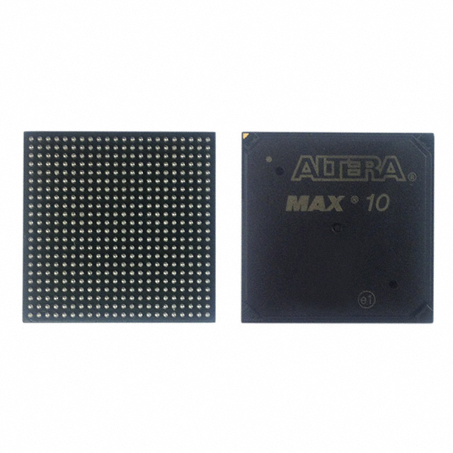
10M08DCF256C7G
| Part Description |
MAX® 10 Field Programmable Gate Array (FPGA) IC 178 387072 8000 256-LBGA |
|---|---|
| Quantity | 58 Available (as of June 14, 2026) |

| Product Category | Field Programmable Gate Array (FPGA) |
|---|---|
| Manufacturer | Intel |
| Manufacturing Status | Obsolete |
| Manufacturer Standard Lead Time | Contact Us |
| Datasheet |
Specifications & Environmental
| Device Package | 256-FBGA (17x17) | Grade | Commercial | Operating Temperature | 0°C – 85°C | ||
|---|---|---|---|---|---|---|---|
| Package / Case | 256-LBGA | Number of I/O | 178 | Voltage | 1.15 V - 1.25 V | ||
| Mounting Method | Surface Mount | RoHS Compliance | Unknown | REACH Compliance | REACH Unaffected | ||
| Moisture Sensitivity Level | 3 (168 Hours) | Number of LABs/CLBs | 500 | Number of Logic Elements/Cells | 8000 | ||
| Number of Gates | N/A | ECCN | 3A991D | HTS Code | 8542.39.0001 | ||
| Qualification | N/A | Total RAM Bits | 387072 |
Overview of 10M08DCF256C7G – MAX® 10 FPGA, 8,000 Logic Elements, 256‑LBGA
The 10M08DCF256C7G is an Intel MAX® 10 field‑programmable gate array (FPGA) supplied in a 256‑ball L‑BGA package. This device provides a mid‑density FPGA fabric with 8,000 logic elements and 500 logic array blocks alongside on‑chip RAM to support a range of configurable digital designs.
With 178 user I/Os, a compact 256‑FBGA (17×17) supplier package, a 1.15–1.25 V core supply range and commercial temperature grading (0 °C to 85 °C), this device targets designs that require balanced logic capacity, memory resources and high I/O density in a surface‑mount form factor.
Key Features
- Core 500 logic array blocks delivering 8,000 logic elements for mid‑density programmable logic implementations.
- On‑Chip Memory Total RAM of 387,072 bits to support state storage, buffering and small lookup tables directly in the FPGA fabric.
- I/O 178 general‑purpose I/O pins to enable dense external interfacing and parallel connectivity in compact designs.
- Power Core supply voltage specified at 1.15 V to 1.25 V to match system power rails and design constraints.
- Package & Mounting 256‑LBGA package (supplier device package: 256‑FBGA, 17×17) optimized for surface‑mount assembly in space‑constrained PCBs.
- Temperature & Grade Commercial grade operation with an operating temperature range of 0 °C to 85 °C.
- Compliance RoHS compliant for materials and manufacturing process considerations.
Typical Applications
- Embedded Control Use the 8,000 logic elements and on‑chip RAM to implement control logic, state machines and peripheral glue for embedded systems.
- I/O Expansion & Interface Bridging Leverage 178 I/Os to bridge parallel and serial interfaces, aggregate signals or implement custom protocol adapters.
- Prototyping & Evaluation Compact package and mid‑density resources make this device suitable for hardware prototyping and proof‑of‑concept FPGA designs.
Unique Advantages
- Balanced Logic and Memory: 8,000 logic elements paired with 387,072 bits of RAM provide the capacity for moderate complexity designs without oversized die cost.
- High I/O Density: 178 user I/Os enable extensive external connectivity in a single device, reducing the need for additional interface ICs.
- Compact Surface‑Mount Package: 256‑LBGA / 256‑FBGA (17×17) package supports dense PCB layouts while remaining compatible with standard surface‑mount assembly.
- Controlled Power Envelope: Defined 1.15–1.25 V core supply simplifies power sequencing and integration with system rails.
- Commercial Temperature Range: Rated for 0 °C to 85 °C operation, matching typical commercial‑grade electronics requirements.
- RoHS Compliant: Conforms to RoHS requirements for material compliance and environmental considerations.
Why Choose 10M08DCF256C7G?
The 10M08DCF256C7G positions itself as a compact, mid‑density FPGA option for designs that need a blend of programmable logic, embedded RAM and substantial I/O in a surface‑mount package. Its 8,000 logic elements, 387,072 bits of RAM and 178 I/Os make it suitable for developers looking to consolidate glue logic, interface functions and custom control into a single FPGA device.
This device suits teams and projects that prioritize integration and board‑level density while operating within commercial temperature ranges and standard power rails. Its package and compliance attributes support efficient assembly and environmental considerations for mainstream electronic products.
Request a quote or submit a pricing and availability inquiry to discuss quantities, lead times and any additional technical requirements for the 10M08DCF256C7G.


Date Founded: 1968
Headquarters: Santa Clara, California, USA
Employees: 130,000+
Revenue: $54.23 Billion
Certifications and Memberships: ISO9001:2015, ISO14001:2015, ISO17025:2017, ISO27001:2022, ISO45001:2018, ISO50001:2018


