
10M25SCE144C8G
| Part Description |
MAX® 10 Field Programmable Gate Array (FPGA) IC 101 691200 25000 144-LQFP Exposed Pad |
|---|---|
| Quantity | 751 Available (as of June 16, 2026) |

| Product Category | Field Programmable Gate Array (FPGA) |
|---|---|
| Manufacturer | Intel |
| Manufacturing Status | Active |
| Manufacturer Standard Lead Time | 16 Weeks |
| Datasheet |
Specifications & Environmental
| Device Package | 144-EQFP (20x20) | Grade | Commercial | Operating Temperature | 0°C – 85°C | ||
|---|---|---|---|---|---|---|---|
| Package / Case | 144-LQFP Exposed Pad | Number of I/O | 101 | Voltage | 2.85 V - 3.465 V | ||
| Mounting Method | Surface Mount | RoHS Compliance | RoHS Compliant | REACH Compliance | REACH Unaffected | ||
| Moisture Sensitivity Level | 3 (168 Hours) | Number of LABs/CLBs | 1563 | Number of Logic Elements/Cells | 25000 | ||
| Number of Gates | N/A | ECCN | 3A991D | HTS Code | 8542.39.0001 | ||
| Qualification | N/A | Total RAM Bits | 691200 |
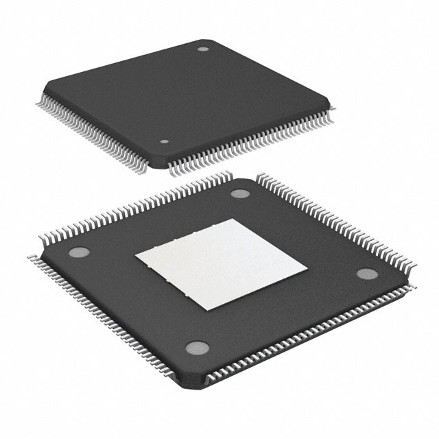
Overview of 10M25SCE144C8G – MAX® 10 FPGA, 25,000 logic elements, 144‑LQFP
The 10M25SCE144C8G is an Intel MAX® 10 Field Programmable Gate Array (FPGA) in a 144‑LQFP exposed‑pad, surface‑mount package. It delivers 25,000 logic elements, 691,200 bits of on‑chip RAM and 101 usable I/O pins in a commercial‑grade device designed for programmable logic and embedded control applications.
This device operates from a 2.85 V to 3.465 V supply and is specified for 0 °C to 85 °C operation. It is RoHS‑compliant and intended for surface‑mount assembly in compact PCB implementations.
Key Features
- Logic Capacity 25,000 logic elements provide programmable logic resources for custom control, glue‑logic and datapath implementation.
- On‑chip Memory 691,200 total RAM bits for embedded buffering, small data stores and state machine storage without external memory.
- Programmable I/O 101 I/O pins enable multiple peripheral interfaces and signal connections directly from the device.
- Package & Mounting 144‑LQFP exposed pad (supplier package listed as 144‑EQFP, 20×20) in a surface‑mount form factor for compact board layouts and thermal coupling through the exposed pad.
- Supply Voltage Operates from 2.85 V to 3.465 V, matching common 3.3 V‑class system rails.
- Operating Temperature Rated for commercial use from 0 °C to 85 °C.
- Compliance RoHS‑compliant construction for regulatory compatibility.
Typical Applications
- Embedded Control Implement custom state machines, timing logic and control interfaces using the device’s logic elements and I/O resources.
- Protocol Bridging & I/O Expansion Use the 101 I/O pins to route and translate signals between subsystems without additional discrete glue logic.
- On‑chip Data Buffering Leverage 691,200 bits of RAM for packet buffering, FIFOs or small local storage to reduce external memory requirements.
- Prototyping & Development Compact LQFP packaging and surface‑mount mounting make the device suitable for board‑level prototypes and proof‑of‑concept designs.
Unique Advantages
- Substantial logic in a compact package: 25,000 logic elements in a 144‑LQFP exposed‑pad package help keep PCB footprint small while providing substantial programmable capability.
- On‑chip RAM reduces BOM: 691,200 bits of internal RAM lower or eliminate the need for external memory in many buffering and state storage use cases.
- Flexible I/O count: 101 I/O pins offer design flexibility for connecting peripherals, sensors and control signals directly to the FPGA.
- Surface‑mount thermal path: Exposed‑pad LQFP package supports improved board thermal coupling and simplified assembly for surface‑mount production.
- Commercial temperature rating: Specified for 0 °C to 85 °C operation to match a wide range of commercial electronics applications.
- RoHS‑compliant: Built to meet RoHS requirements for environmentally compliant designs.
Why Choose 10M25SCE144C8G?
The 10M25SCE144C8G provides a balanced combination of programmable logic capacity, on‑chip RAM and I/O density in a compact surface‑mount package. Its electrical and package specifications make it well suited for commercial embedded designs that require integrated logic, local memory and a flexible I/O count without expanding board area or BOM complexity.
This device is appropriate for designers seeking a commercially rated Intel MAX 10 FPGA with clear supply and temperature specifications, straightforward board mounting (144‑LQFP exposed pad) and RoHS compliance for production deployment.
Request a quote or submit an inquiry for pricing, availability and lead‑time information for the 10M25SCE144C8G.


Date Founded: 1968
Headquarters: Santa Clara, California, USA
Employees: 130,000+
Revenue: $54.23 Billion
Certifications and Memberships: ISO9001:2015, ISO14001:2015, ISO17025:2017, ISO27001:2022, ISO45001:2018, ISO50001:2018


