
10M40DAF256C8G
| Part Description |
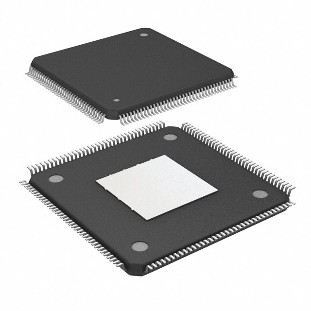
MAX® 10 Field Programmable Gate Array (FPGA) IC 178 1290240 40000 256-LBGA |
|---|---|
| Quantity | 1,076 Available (as of June 10, 2026) |

| Product Category | Field Programmable Gate Array (FPGA) |
|---|---|
| Manufacturer | Intel |
| Manufacturing Status | Active |
| Manufacturer Standard Lead Time | 16 Weeks |
| Datasheet |
Specifications & Environmental
| Device Package | 256-FBGA (17x17) | Grade | Commercial | Operating Temperature | 0°C – 85°C | ||
|---|---|---|---|---|---|---|---|
| Package / Case | 256-LBGA | Number of I/O | 178 | Voltage | 1.15 V - 1.25 V | ||
| Mounting Method | Surface Mount | RoHS Compliance | RoHS Compliant | REACH Compliance | REACH Unaffected | ||
| Moisture Sensitivity Level | 3 (168 Hours) | Number of LABs/CLBs | 2500 | Number of Logic Elements/Cells | 40000 | ||
| Number of Gates | N/A | ECCN | 3A991D | HTS Code | 8542.39.0001 | ||
| Qualification | N/A | Total RAM Bits | 1290240 |
Overview of 10M40DAF256C8G – MAX® 10 Field Programmable Gate Array (FPGA) IC 178 1290240 40000 256-LBGA
The 10M40DAF256C8G is an Intel MAX® 10 FPGA device supplied in a 256-LBGA package. It integrates 40,000 logic elements, 1,290,240 bits of on-chip RAM and up to 178 I/O pins in a surface-mount BGA footprint for compact commercial designs.
Designed for commercial embedded applications, this MAX 10 device delivers a balance of logic density, on-chip memory and flexible I/O while operating from a 1.15 V to 1.25 V supply and across a 0 °C to 85 °C temperature range. The device is RoHS compliant and follows the MAX 10 device family specification for configuration and timing.
Key Features
- Core Logic 40,000 logic elements (logic cells) for implementing combinational and sequential logic functionality at moderate to high capacity.
- On‑Chip Memory 1,290,240 total RAM bits provide substantial embedded memory for FIFOs, buffering and local data storage without external memory.
- I/O Capacity & Flexibility Up to 178 I/O pins support a variety of parallel and serial interfacing requirements; the MAX 10 datasheet documents programmable I/O delay features for timing tuning.
- Power & Core Voltage Core supply voltage range of 1.15 V to 1.25 V for low‑voltage operation consistent with modern FPGA power domains.
- Package & Mounting 256‑LBGA package (supplier package: 256‑FBGA 17×17) in a surface-mount form factor to minimize board area and support compact PCB layouts.
- Operating Range & Grade Commercial grade device with an operating temperature range of 0 °C to 85 °C suitable for standard commercial environments.
- Configuration & Test Device documentation includes configuration specifications and JTAG timing parameters as part of the Intel MAX 10 FPGA device datasheet.
- Standards Compliance RoHS compliant to meet environmental and manufacturing requirements for lead‑free production.
Typical Applications
- Commercial Embedded Systems Integration of control logic, protocol bridging and custom processing in space-constrained, commercial electronic products using the device's logic density and on-chip RAM.
- Communications and Interface Bridging Implement protocol converters, interface glue logic or packet buffering leveraging up to 178 I/O pins and substantial RAM resources.
- Consumer Electronics Feature control, sensor aggregation and user‑interface handling in consumer devices where a compact 256‑LBGA package and surface‑mount mounting are beneficial.
- Prototyping and Development Hardware validation, algorithm acceleration and proof‑of‑concept designs that require reprogrammable logic, on-chip RAM and standard configuration/JTAG support.
Unique Advantages
- High Logic Capacity: 40,000 logic elements enable implementation of substantial custom logic without immediate need for larger discrete FPGA families.
- Large On‑Chip RAM: 1,290,240 bits of embedded RAM reduce or eliminate dependence on external memory for many buffering and storage tasks.
- Flexible I/O Count: 178 I/O pins provide headroom for multiple peripherals, buses and interface requirements on a single device.
- Compact BGA Package: 256‑LBGA (256‑FBGA 17×17) minimizes PCB area while providing a high pin count for dense designs.
- Low‑Voltage Core Operation: 1.15 V to 1.25 V supply range supports modern low-voltage system designs.
- Commercial Temperature Rating & RoHS Compliance: Rated 0 °C to 85 °C and RoHS compliant for mainstream commercial products and manufacturing flows.
Why Choose 10M40DAF256C8G?
The 10M40DAF256C8G positions itself as a commercially graded, mid-to-high density FPGA option within the Intel MAX 10 family, combining 40,000 logic elements, more than 1.29 Mb of on-chip RAM and up to 178 I/O in a compact 256‑LBGA package. Its low-voltage core and documented configuration and JTAG timing characteristics make it a practical choice for commercial embedded designs that require integrated memory and flexible interfacing without external components.
This device is suitable for design teams looking to consolidate logic and buffering into a single programmable device while maintaining a compact board footprint and standard commercial temperature operation. The MAX 10 datasheet provides detailed electrical, configuration and timing information required for system integration and validation.
Request a quote or submit an RFQ to get pricing, availability and lead-time information for the 10M40DAF256C8G FPGA.


Date Founded: 1968
Headquarters: Santa Clara, California, USA
Employees: 130,000+
Revenue: $54.23 Billion
Certifications and Memberships: ISO9001:2015, ISO14001:2015, ISO17025:2017, ISO27001:2022, ISO45001:2018, ISO50001:2018


