
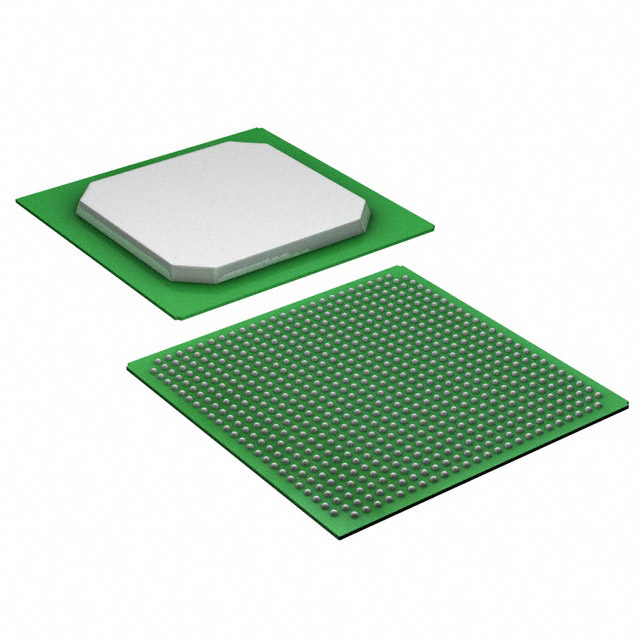
10M40DCF484C8G
| Part Description |
MAX® 10 Field Programmable Gate Array (FPGA) IC 360 1290240 40000 484-BGA |
|---|---|
| Quantity | 690 Available (as of June 14, 2026) |

| Product Category | Field Programmable Gate Array (FPGA) |
|---|---|
| Manufacturer | Intel |
| Manufacturing Status | Active |
| Manufacturer Standard Lead Time | 12 Weeks |
| Datasheet |
Specifications & Environmental
| Device Package | 484-FBGA (23x23) | Grade | Commercial | Operating Temperature | 0°C – 85°C | ||
|---|---|---|---|---|---|---|---|
| Package / Case | 484-BGA | Number of I/O | 360 | Voltage | 1.15 V - 1.25 V | ||
| Mounting Method | Surface Mount | RoHS Compliance | RoHS Compliant | REACH Compliance | REACH Unaffected | ||
| Moisture Sensitivity Level | 3 (168 Hours) | Number of LABs/CLBs | 2500 | Number of Logic Elements/Cells | 40000 | ||
| Number of Gates | N/A | ECCN | 3A001A7A | HTS Code | 8542.39.0001 | ||
| Qualification | N/A | Total RAM Bits | 1290240 |
Overview of 10M40DCF484C8G – MAX® 10 Field Programmable Gate Array (FPGA) IC 360 1290240 40000 484-BGA
The 10M40DCF484C8G is a MAX® 10 Field Programmable Gate Array (FPGA) IC from Intel, provided in a 484-ball FBGA package. It combines a mid-scale logic resource set with substantial on-chip RAM and a high I/O count, optimized for commercial-grade embedded designs operating at standard commercial temperatures.
Designed for applications that require configurable digital logic, abundant on-chip memory, and dense external connectivity, this device supports integration of custom control, interface, and processing functions while operating from a 1.15 V to 1.25 V supply.
Key Features
- Core Logic Approximately 40,000 logic elements provide a mid-range programmable fabric for implementing custom digital functions and control logic.
- On‑Chip Memory Total on-chip RAM of 1,290,240 bits enables local buffering, look‑up tables, and memory-mapped logic without immediate dependence on external memory.
- I/O Density 360 available I/O pins support high pin-count interfaces and multiple parallel connections to peripherals and sensors.
- Power Core supply range of 1.15 V to 1.25 V provides a defined operating window for power delivery and board-level design considerations.
- Package and Mounting 484-ball FBGA (23 × 23) package in a 484‑BGA footprint, intended for surface-mount assembly to support compact board layouts.
- Operating Range Commercial-grade operating temperature from 0 °C to 85 °C, suitable for typical commercial and consumer electronic environments.
- Regulatory RoHS compliant, supporting lead‑free and environmentally conscious manufacturing processes.
Typical Applications
- Interface and Connectivity Modules High I/O count supports implementation of multi‑lane interfaces, protocol bridging, and custom peripheral expansions.
- Embedded Control Systems Logic capacity and on-chip RAM enable implementation of control algorithms, state machines, and real-time decision logic in commercial products.
- Data Buffering and Packet Processing Substantial on-chip RAM supports local buffering and packet handling for mid-rate data-processing tasks.
Unique Advantages
- Balanced Logic and Memory: The combination of ~40,000 logic elements and 1,290,240 bits of RAM provides designers with both programmable logic resources and on-chip storage for compact, integrated designs.
- High I/O Count: 360 I/O pins allow direct connection to multiple peripherals and parallel buses, reducing the need for external multiplexing or I/O expanders.
- Compact Package: The 484‑FBGA (23 × 23) package supports dense PCB implementations while maintaining a surface-mount footprint suitable for modern assemblies.
- Commercial Temperature Suitability: Rated for 0 °C to 85 °C operation, it is appropriate for consumer and commercial applications with standard environmental requirements.
- Defined Power Envelope: A specified supply range of 1.15 V to 1.25 V helps streamline power-supply design and validation for the FPGA core.
- RoHS Compliance: Environmentally compliant manufacturing compatibility simplifies integration into lead‑free product lines.
Why Choose 10M40DCF484C8G?
The 10M40DCF484C8G positions itself as a mid-range, commercially rated MAX® 10 FPGA that balances programmable logic capacity, significant on-chip memory, and a large I/O complement in a compact 484‑FBGA package. Its electrical and thermal specifications make it suitable for commercial embedded systems where configurable logic, local RAM, and dense connectivity are required.
This device is appropriate for designers and procurement teams building commercial electronic products that need flexible hardware programmability with clear parameters for power, temperature, and packaging. Its combination of resources supports scalable designs that can consolidate functions and reduce external component count.
Request a quote or submit an inquiry to receive pricing, availability, and ordering information for the 10M40DCF484C8G.


Date Founded: 1968
Headquarters: Santa Clara, California, USA
Employees: 130,000+
Revenue: $54.23 Billion
Certifications and Memberships: ISO9001:2015, ISO14001:2015, ISO17025:2017, ISO27001:2022, ISO45001:2018, ISO50001:2018


