
10M50DAF256C8G
| Part Description |
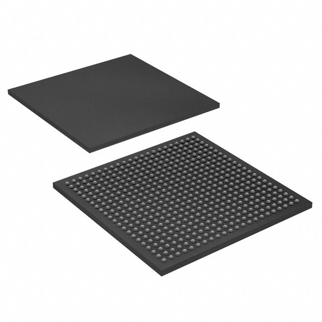
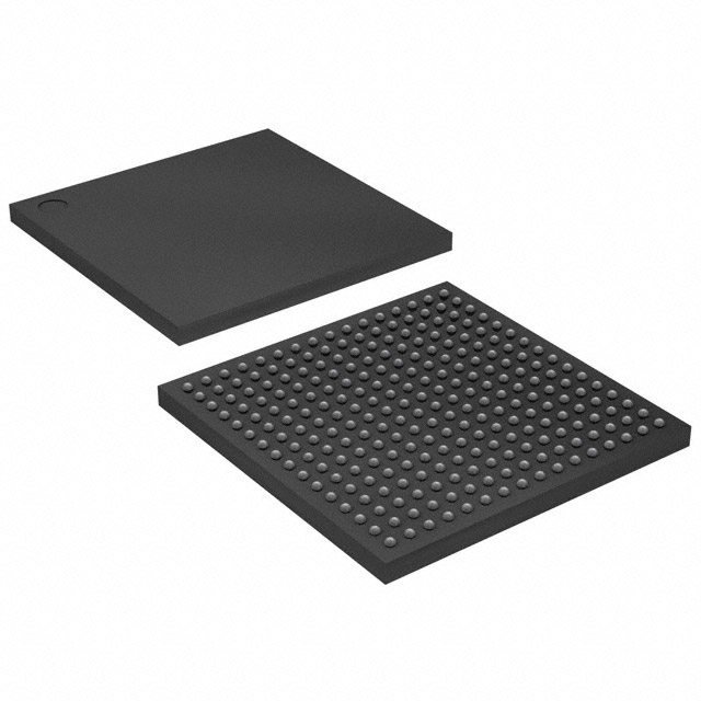
MAX® 10 Field Programmable Gate Array (FPGA) IC 178 1677312 50000 256-LBGA |
|---|---|
| Quantity | 120 Available (as of June 15, 2026) |

| Product Category | Field Programmable Gate Array (FPGA) |
|---|---|
| Manufacturer | Intel |
| Manufacturing Status | Active |
| Manufacturer Standard Lead Time | 16 Weeks |
| Datasheet |
Specifications & Environmental
| Device Package | 256-FBGA (17x17) | Grade | Commercial | Operating Temperature | 0°C – 85°C | ||
|---|---|---|---|---|---|---|---|
| Package / Case | 256-LBGA | Number of I/O | 178 | Voltage | 1.15 V - 1.25 V | ||
| Mounting Method | Surface Mount | RoHS Compliance | RoHS Compliant | REACH Compliance | REACH Unaffected | ||
| Moisture Sensitivity Level | 3 (168 Hours) | Number of LABs/CLBs | 3125 | Number of Logic Elements/Cells | 50000 | ||
| Number of Gates | N/A | ECCN | 3A991D | HTS Code | 8542.39.0001 | ||
| Qualification | N/A | Total RAM Bits | 1677312 |
Overview of 10M50DAF256C8G – MAX® 10 FPGA, 50,000 Logic Elements, 256-LBGA
The 10M50DAF256C8G is an Intel MAX® 10 field programmable gate array (FPGA) supplied in a 256-ball L-BGA package. It integrates 50,000 logic elements and 1,677,312 total RAM bits with 178 general-purpose I/Os, delivering a compact, reconfigurable silicon element for commercial embedded designs.
Targeted at commercial applications, this device provides a balance of on-chip logic density, on-chip memory, and I/O capacity while operating from a 1.15 V to 1.25 V supply and across a 0 °C to 85 °C ambient range.
Key Features
- Core Logic — 50,000 logic elements providing substantial programmable fabric for custom digital functions and control logic.
- Memory — 1,677,312 total RAM bits to support buffering, packet processing, and state storage inside the FPGA fabric.
- I/O Capability — 178 I/O pins that enable connectivity to multiple external peripherals, sensors, and interface modules.
- Power — Operates from a core voltage supply range of 1.15 V to 1.25 V, suitable for designs specifying a defined core power budget.
- Package — 256-LBGA (256-FBGA, 17 × 17) package for compact board-level integration and reliable surface-mount assembly.
- Operating Range — Commercial temperature grade with an operating range of 0 °C to 85 °C for standard commercial electronics deployments.
- Compliance — RoHS compliant, meeting common environmental and materials restrictions for electronic products.
Typical Applications
- Custom Logic and Prototyping — Implement custom digital logic, glue logic, and rapid prototypes using the device’s 50,000 logic elements and abundant on-chip RAM.
- I/O-Intensive Interfaces — Use the 178 I/Os to bridge multiple external peripherals, parallel buses, or mixed-signal front ends in embedded systems.
- Embedded Control and Signal Processing — Leverage the on-chip RAM and logic resources to implement control loops, data buffering, and basic signal processing tasks for commercial products.
Unique Advantages
- Substantial On-Chip Logic — 50,000 logic elements enable implementation of complex finite-state machines, data paths, and control logic without external ASICs.
- Generous Embedded Memory — 1,677,312 RAM bits support larger data buffers and local storage, reducing dependence on external memories.
- High I/O Count — 178 I/Os simplify board-level interfacing by accommodating multiple signals and buses directly to the FPGA.
- Space-Efficient Package — 256-LBGA (17 × 17) package offers a compact solution for high-density PCB layouts.
- Commercial Temperature Range — Rated for 0 °C to 85 °C, aligning with typical commercial electronics deployment environments.
- RoHS Compliant — Conforms to materials restrictions for regulatory and supply-chain consistency.
Why Choose 10M50DAF256C8G?
The 10M50DAF256C8G positions itself as a versatile, commercially rated FPGA that balances logic density, on-chip memory, and I/O capacity in a compact 256-LBGA package. Its specification set supports a wide range of embedded and system-level designs that require reconfigurable logic, local RAM, and substantial external interfacing.
Designed and manufactured by Intel, this MAX® 10 device is suitable for commercial design teams seeking a scalable, reprogrammable building block backed by an established FPGA vendor.
Request a quote or submit a pricing inquiry to receive availability and purchasing options for 10M50DAF256C8G.


Date Founded: 1968
Headquarters: Santa Clara, California, USA
Employees: 130,000+
Revenue: $54.23 Billion
Certifications and Memberships: ISO9001:2015, ISO14001:2015, ISO17025:2017, ISO27001:2022, ISO45001:2018, ISO50001:2018


