
1SD110PJ2F43I1VG
| Part Description |
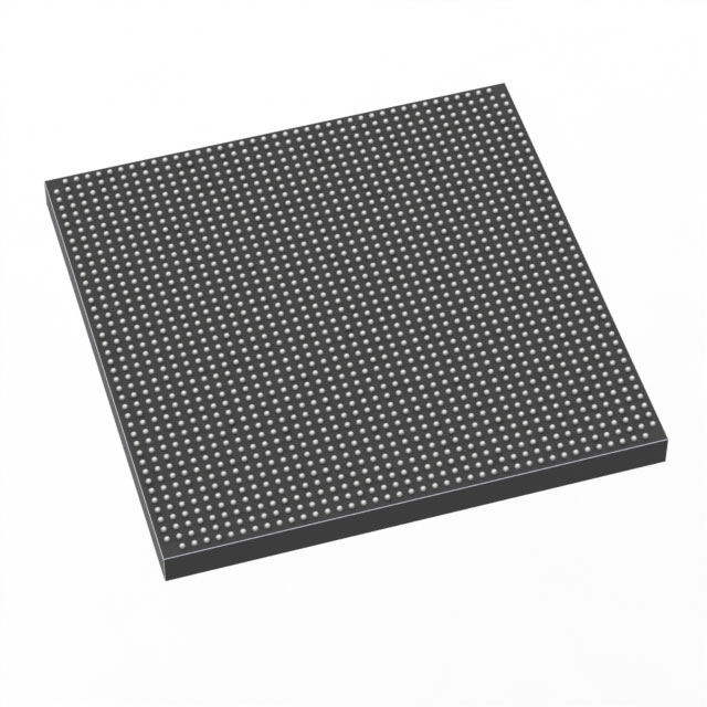
Stratix® 10 DX Field Programmable Gate Array (FPGA) IC 528 112197632 1325000 1760-BBGA, FCBGA |
|---|---|
| Quantity | 1,375 Available (as of October 7, 2026) |

| Product Category | Field Programmable Gate Array (FPGA) |
|---|---|
| Manufacturer | Intel |
| Manufacturing Status | Active |
| Manufacturer Standard Lead Time | 12 Weeks |
| Datasheet |
Specifications & Environmental
| Device Package | 1760-FBGA (42.5x42.5) | Grade | Industrial | Operating Temperature | -40°C – 100°C | ||
|---|---|---|---|---|---|---|---|
| Package / Case | 1760-BBGA, FCBGA | Number of I/O | 528 | Voltage | 870 mV - 970 mV | ||
| Mounting Method | Surface Mount | RoHS Compliance | Unknown | REACH Compliance | REACH Unknown | ||
| Moisture Sensitivity Level | 3 (168 Hours) | Number of LABs/CLBs | N/A | Number of Logic Elements/Cells | 1325000 | ||
| Number of Gates | N/A | ECCN | N/A | HTS Code | N/A | ||
| Qualification | N/A | Total RAM Bits | 112197632 |
Overview of 1SD110PJ2F43I1VG – Stratix® 10 DX Field Programmable Gate Array (FPGA) IC
The 1SD110PJ2F43I1VG is an Intel Stratix 10 DX family FPGA supplied in a 1760-ball FCBGA package. It combines a very large logic capacity and on-chip RAM with industrial-grade temperature capability for demanding embedded and system-level designs.
Targeted at designs that require high logic density, substantial on-chip memory and robust I/O, this device delivers a combination of integration and reliability through specifications such as 1,325,000 logic element cells, 112,197,632 total RAM bits and 528 I/O pins.
Key Features
- Core Capacity 1,325,000 logic element cells provide large programmable fabric for complex logic, custom accelerators and system integration.
- On-chip Memory 112,197,632 total RAM bits enable large data buffering, state storage and memory-hungry processing inside the FPGA fabric.
- I/O 528 user I/O pins support extensive external connectivity for high-bandwidth interfaces and multi-channel designs.
- Power Supply Core voltage range specified at 870 mV to 970 mV allows clear power planning and margining for system power delivery design.
- Package & Mounting 1760-BBGA (1760-FBGA supplier package) with a 42.5 × 42.5 mm footprint, designed for surface-mount assembly and high-density board layouts.
- Operating Environment Industrial-grade operating temperature from −40 °C to 100 °C for deployment in thermally challenging environments.
- Regulatory RoHS-compliant construction for environmental regulatory alignment.
- Family-Level Documentation Device-specific errata and family documentation address system-level behaviors such as PCIe, Hard Processor System and memory interface issues for informed system integration.
Typical Applications
- Embedded SoC and HPS-based Systems Leverages family-level support for Hard Processor System and Arm Cortex‑A53 elements for designs combining programmable logic with embedded processing.
- High-throughput I/O Systems Large I/O count and high logic density suit PCIe-linked or multi-channel I/O applications that require significant interface and protocol logic.
- Memory-intensive Accelerators Substantial on-chip RAM bits allow implementation of on-chip buffering, lookup tables and accelerator state for compute and signal-processing tasks.
Unique Advantages
- High Logic Density: 1,325,000 logic element cells enable consolidation of complex subsystems and custom accelerators into a single device, reducing board-level component count.
- Large On-chip Memory: Over 112 million bits of RAM reduce external memory dependency and improve data-path latency for compute-intensive workloads.
- Extensive I/O: 528 I/O pins allow flexible partitioning of interfaces and parallel channels, simplifying multi-protocol board designs.
- Industrial Temperature Range: Rated −40 °C to 100 °C for deployment in industrial and ruggedized environments where thermal margins are a concern.
- Compact, High-density Package: 1760-FBGA (42.5 × 42.5 mm) facilitates high-density PCB designs while supporting surface-mount assembly processes.
- Documented Family Errata and Guidance: Family-level errata and technical documentation provide visibility into known device behaviors (PCIe, HPS, memory interfaces) to support robust system integration.
Why Choose 1SD110PJ2F43I1VG?
This Stratix 10 DX device positions itself for designs that require a large programmable fabric, substantial on-chip memory and extensive I/O in an industrial-temperature-rated package. The combination of 1,325,000 logic element cells, 112,197,632 RAM bits and 528 I/O pins provides the raw resources needed to integrate complex subsystems and reduce external components.
Engineers building embedded SoC platforms, high-throughput interface systems or memory-intensive accelerators will find the device’s capacity, package density and documented family-level guidance useful for long-term development, scalability and system reliability.
Request a quote or submit a purchase inquiry to receive pricing, availability and lead-time information for 1SD110PJ2F43I1VG. Include your quantity and any specific packaging or procurement requirements to expedite a response.























Date Founded: 1968
Headquarters: Santa Clara, California, USA
Employees: 130,000+
Revenue: $54.23 Billion
Certifications and Memberships: ISO9001:2015, ISO14001:2015, ISO17025:2017, ISO27001:2022, ISO45001:2018, ISO50001:2018


