
1SG040HH1F35E2VG
| Part Description |
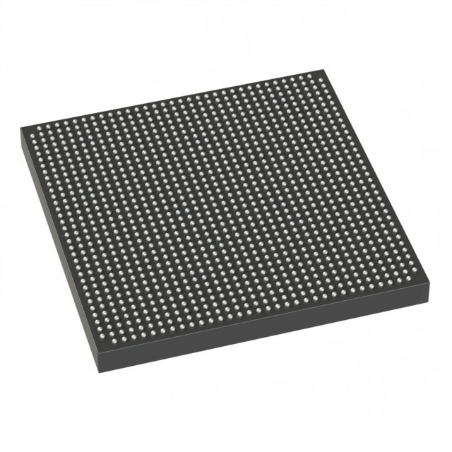
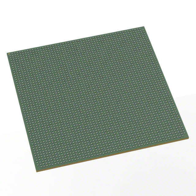
Stratix® 10 GX Field Programmable Gate Array (FPGA) IC 374 31457280 378000 1152-BBGA, FCBGA |
|---|---|
| Quantity | 498 Available (as of June 10, 2026) |
| Product Category | Field Programmable Gate Array (FPGA) |
|---|---|
| Manufacturer | Intel |
| Manufacturing Status | Active |
| Manufacturer Standard Lead Time | 12 Weeks |
| Datasheet |
Specifications & Environmental
| Device Package | 1152-FBGA (35x35) | Grade | Extended | Operating Temperature | 0°C – 100°C | ||
|---|---|---|---|---|---|---|---|
| Package / Case | 1152-BBGA, FCBGA | Number of I/O | 374 | Voltage | 770 mV - 970 mV | ||
| Mounting Method | Surface Mount | RoHS Compliance | Unknown | REACH Compliance | REACH Unknown | ||
| Moisture Sensitivity Level | 3 (168 Hours) | Number of LABs/CLBs | 47250 | Number of Logic Elements/Cells | 378000 | ||
| Number of Gates | N/A | ECCN | N/A | HTS Code | N/A | ||
| Qualification | N/A | Total RAM Bits | 31457280 |
Overview of 1SG040HH1F35E2VG – Stratix® 10 GX FPGA, 378,000 logic elements, 1152-FBGA (35×35)
The 1SG040HH1F35E2VG is a Stratix® 10 GX Field Programmable Gate Array (FPGA) device offering a large logic fabric and substantial on-chip memory. It combines 378,000 logic elements, 31,457,280 bits of RAM and 374 I/O in a 1152-FBGA (35×35) surface-mount package.
This Extended-grade FPGA operates over a 770 mV to 970 mV supply range and is specified for 0 °C to 100 °C environments, making it suitable for designs that require high logic density, significant embedded memory, and a high I/O count in a compact footprint.
Key Features
- Core Logic 378,000 logic elements provide large-scale programmable logic capacity for complex designs and integration of multiple functions on a single device.
- On-Chip Memory 31,457,280 total RAM bits available for data buffering, intermediate storage, and memory-intensive processing without immediate reliance on external memory.
- I/O Capacity 374 I/O pins enable broad connectivity options for peripherals, sensors, and board-level interfaces.
- Package & Mounting 1152-BBGA, FCBGA (1152-FBGA, 35×35) surface-mount package delivers a compact, board-level footprint for high-density designs.
- Power Supports a core voltage supply range from 770 mV to 970 mV to match system power-domain requirements.
- Temperature & Grade Extended grade device rated for operation from 0 °C to 100 °C.
- Regulatory RoHS compliant.
Typical Applications
- High-density digital processing — Implement large custom logic blocks and complex finite-state machines using the device’s 378,000 logic elements and extensive on-chip RAM.
- Multi-I/O system integration — Aggregate and route signals from numerous peripherals or subsystems using the 374 available I/O.
- Embedded acceleration — Offload compute-heavy kernels and buffering tasks to dedicated logic and on-chip RAM to reduce external memory dependence.
- Compact system boards — Integrate substantial functionality in designs constrained by board area using the 1152-FBGA (35×35) package.
Unique Advantages
- Significant logic capacity: 378,000 logic elements allow consolidation of multiple functions and large custom architectures onto a single FPGA.
- Large on-chip memory: 31,457,280 bits of RAM reduce the need for external memory for many buffering and state-storage tasks.
- High I/O count: 374 I/O pins provide flexibility to connect multiple peripherals, sensors, and interfaces without additional I/O expanders.
- Compact FCBGA package: The 1152-FBGA (35×35) footprint enables dense board layouts while keeping package-level routing predictable.
- Power-domain compatibility: Core operation across 770 mV to 970 mV supports designs with low-voltage power architectures.
- Extended-grade rating: Rated for 0 °C to 100 °C operation to support deployments outside of narrow commercial temperature ranges.
Why Choose 1SG040HH1F35E2VG?
The 1SG040HH1F35E2VG delivers a balance of high logic density, substantial on-chip RAM, and a broad I/O complement in a compact 1152-FBGA package. Its Extended-grade specification and defined supply range make it appropriate for designs that need integrated capability and predictable electrical characteristics.
Designers targeting complex, memory-aware logic implementations or systems requiring many external connections will find the device’s combination of logic elements, RAM, and I/O advantageous for reducing board-level complexity and consolidating functions into a single FPGA.
Request a quote or submit an inquiry to receive pricing, availability, and additional ordering information for this Stratix® 10 GX FPGA.


Date Founded: 1968
Headquarters: Santa Clara, California, USA
Employees: 130,000+
Revenue: $54.23 Billion
Certifications and Memberships: ISO9001:2015, ISO14001:2015, ISO17025:2017, ISO27001:2022, ISO45001:2018, ISO50001:2018


