
1SG040HH2F35I2LG
| Part Description |
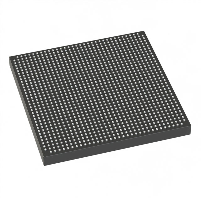
Stratix® 10 GX Field Programmable Gate Array (FPGA) IC 374 31457280 378000 1152-BBGA, FCBGA |
|---|---|
| Quantity | 1,174 Available (as of June 18, 2026) |

| Product Category | Field Programmable Gate Array (FPGA) |
|---|---|
| Manufacturer | Intel |
| Manufacturing Status | Active |
| Manufacturer Standard Lead Time | 12 Weeks |
| Datasheet |
Specifications & Environmental
| Device Package | 1152-FBGA (35x35) | Grade | Industrial | Operating Temperature | -40°C – 100°C | ||
|---|---|---|---|---|---|---|---|
| Package / Case | 1152-BBGA, FCBGA | Number of I/O | 374 | Voltage | 820 mV - 880 mV | ||
| Mounting Method | Surface Mount | RoHS Compliance | Unknown | REACH Compliance | REACH Unknown | ||
| Moisture Sensitivity Level | 3 (168 Hours) | Number of LABs/CLBs | 47250 | Number of Logic Elements/Cells | 378000 | ||
| Number of Gates | N/A | ECCN | N/A | HTS Code | N/A | ||
| Qualification | N/A | Total RAM Bits | 31457280 |
Overview of 1SG040HH2F35I2LG – Stratix® 10 GX FPGA, 378000 Logic Elements, 31,457,280‑bit RAM, 374 I/O
The 1SG040HH2F35I2LG is a Stratix® 10 GX Field Programmable Gate Array (FPGA) IC. It provides a high logic‑density FPGA fabric with on‑chip RAM and a large number of I/O pins in a 1152‑BBGA FCBGA package.
With 378,000 logic elements, 31,457,280 total RAM bits and 374 I/O, the device targets designs that require substantial programmable logic, embedded memory and broad external connectivity while operating across an industrial temperature range.
Key Features
- Core Logic 378,000 logic elements for implementing complex digital logic and large-scale custom hardware functions.
- On‑Chip Memory 31,457,280 total RAM bits to support data buffering, lookup tables and state storage within the FPGA fabric.
- I/O Density 374 I/O pins to enable extensive board‑level interfacing and connectivity to external devices and subsystems.
- Power Supply Specified supply voltage range from 820 mV to 880 mV for core power planning and regulator selection.
- Package & Mounting 1152‑BBGA (FCBGA) package, supplier device package 1152‑FBGA (35×35), surface‑mount component suitable for compact board designs.
- Temperature & Grade Industrial grade device rated for operation from −40 °C to 100 °C for systems requiring extended temperature capability.
- Compliance RoHS‑compliant material status to support environmental regulatory requirements.
Typical Applications
- Custom Hardware Acceleration Use the high logic element count and large on‑chip RAM to implement application‑specific accelerators and parallel processing blocks.
- High‑Density Interface Aggregation Leverage 374 I/O pins to aggregate and bridge multiple external interfaces or to connect large sensor and actuator arrays.
- Industrial Control & Automation Industrial temperature rating and robust packaging make the device suitable for control systems and automation equipment operating across wide temperature ranges.
Unique Advantages
- High Logic Capacity: 378,000 logic elements enable complex, large‑scale FPGA designs without immediate need for multi‑device partitioning.
- Substantial On‑Chip RAM: 31,457,280 bits of RAM reduce reliance on external memory for buffering and state storage, simplifying system memory architecture.
- Extensive I/O Count: 374 I/O pins provide flexibility for routing multiple peripherals, high‑channel count systems or extensive board interconnects.
- Industrial Temperature Range: −40 °C to 100 °C rating supports deployment in temperature‑stressed environments common in industrial applications.
- Compact BGA Packaging: 1152‑BBGA (35×35) surface‑mount package balances high pin count with a compact board footprint for space‑constrained designs.
- Regulatory Compliance: RoHS compliance aids in meeting environmental requirements during manufacturing and deployment.
Why Choose 1SG040HH2F35I2LG?
The 1SG040HH2F35I2LG combines high logic density, extensive on‑chip memory and broad I/O capability in a compact 1152‑BBGA package with industrial temperature capability. This combination positions the device for designs that need significant programmable resources and robust board‑level connectivity while operating in demanding temperature environments.
Engineers and procurement teams seeking a scalable, high‑capacity FPGA solution will find this device suitable for complex digital implementations where on‑chip RAM and I/O count directly impact architecture choices and system integration.
Request a quote or submit an inquiry to receive pricing and availability for 1SG040HH2F35I2LG.


Date Founded: 1968
Headquarters: Santa Clara, California, USA
Employees: 130,000+
Revenue: $54.23 Billion
Certifications and Memberships: ISO9001:2015, ISO14001:2015, ISO17025:2017, ISO27001:2022, ISO45001:2018, ISO50001:2018


