
1SG065HH1F35E2LG
| Part Description |
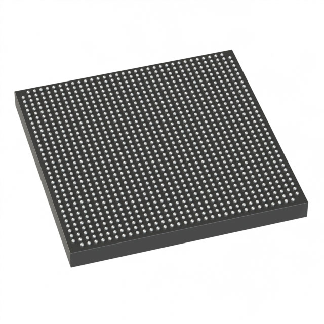
Stratix® 10 GX Field Programmable Gate Array (FPGA) IC 392 51380224 612000 1152-BBGA, FCBGA |
|---|---|
| Quantity | 1,786 Available (as of June 10, 2026) |

| Product Category | Field Programmable Gate Array (FPGA) |
|---|---|
| Manufacturer | Intel |
| Manufacturing Status | Active |
| Manufacturer Standard Lead Time | 12 Weeks |
| Datasheet |
Specifications & Environmental
| Device Package | 1152-FBGA (35x35) | Grade | Extended | Operating Temperature | 0°C – 100°C | ||
|---|---|---|---|---|---|---|---|
| Package / Case | 1152-BBGA, FCBGA | Number of I/O | 392 | Voltage | 820 mV - 880 mV | ||
| Mounting Method | Surface Mount | RoHS Compliance | Unknown | REACH Compliance | REACH Unknown | ||
| Moisture Sensitivity Level | 3 (168 Hours) | Number of LABs/CLBs | 76500 | Number of Logic Elements/Cells | 612000 | ||
| Number of Gates | N/A | ECCN | N/A | HTS Code | N/A | ||
| Qualification | N/A | Total RAM Bits | 51380224 |
Overview of 1SG065HH1F35E2LG – Stratix® 10 GX Field Programmable Gate Array (FPGA) IC
The 1SG065HH1F35E2LG is an Intel Stratix® 10 GX Field Programmable Gate Array (FPGA) IC designed for high-density digital designs. It integrates a large logic fabric, extensive on-chip memory, and a high I/O count in a compact ball-grid array package.
Key device attributes include 612,000 logic elements, 51,380,224 total RAM bits, and 392 I/O. The device ships in a 1152-BBGA (1152-FBGA, 35×35) surface-mount package, operates from a core supply of 820 mV to 880 mV, and is specified for 0 °C to 100 °C operating temperature. Grade is Extended and the part is RoHS compliant.
Key Features
- Core Logic — 612,000 logic elements provide substantial capacity for complex combinational and sequential logic implementations.
- On-chip Memory — 51,380,224 total RAM bits for buffering, frame storage, and local data processing without relying solely on external memory.
- I/O Resources — 392 I/O pins enable wide parallel interfaces and multi-channel connectivity for system-level integration.
- Power — Core voltage supply range of 820 mV to 880 mV for precise power budgeting and supply sequencing.
- Package & Mounting — 1152-BBGA (Supplier Device Package: 1152-FBGA, 35×35) surface-mount package for high-density board designs.
- Temperature & Grade — Operating temperature range of 0 °C to 100 °C; device grade is Extended.
- Compliance — RoHS compliant.
Typical Applications
- High-density digital signal processing — Large logic capacity and abundant on-chip RAM support implementation of complex DSP pipelines and parallel processing engines.
- Custom hardware acceleration — High logic and memory resources enable creation of application-specific accelerators for compute-intensive tasks.
- Multi-channel I/O and protocol bridging — 392 I/O pins facilitate wide data buses, protocol conversion, and multi-lane interfacing on a single device.
Unique Advantages
- Large programmable fabric: 612,000 logic elements let you implement sizable, integrated designs without partitioning across multiple FPGAs.
- Extensive on-chip memory: 51,380,224 RAM bits reduce dependence on external memory for buffering and state storage, simplifying board design.
- High I/O count: 392 I/O enables flexible system interfacing and supports complex connectivity needs on a single package.
- Compact, high-density package: 1152-BBGA (35×35) surface-mount packaging conserves PCB area while supporting high pin counts.
- Predictable power envelope: Narrow core voltage range (820 mV–880 mV) supports focused power-supply design and thermal planning.
- Extended operating grade and RoHS compliance: 0 °C to 100 °C operating range with Extended grade and environmental compliance for a range of deployments.
Why Choose 1SG065HH1F35E2LG?
The 1SG065HH1F35E2LG combines very large logic capacity, substantial on-chip RAM, and a high I/O count in a compact 1152-ball BGA package, making it well suited for designers who need to consolidate complex digital functions into a single FPGA. Its defined core voltage range, extended operating grade, and RoHS compliance support disciplined power and thermal planning for production designs.
This device is appropriate for development teams building high-density signal processing, custom acceleration, or multi-interface systems that benefit from integrated logic and memory resources within a surface-mount BGA footprint.
Request a quote or submit an inquiry to obtain pricing, availability, and lead-time information for 1SG065HH1F35E2LG.


Date Founded: 1968
Headquarters: Santa Clara, California, USA
Employees: 130,000+
Revenue: $54.23 Billion
Certifications and Memberships: ISO9001:2015, ISO14001:2015, ISO17025:2017, ISO27001:2022, ISO45001:2018, ISO50001:2018


