
1SG110HN3F43I3VGAS
| Part Description |
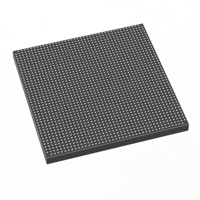
Stratix® 10 GX Field Programmable Gate Array (FPGA) IC 688 1100000 1760-BBGA, FCBGA |
|---|---|
| Quantity | 425 Available (as of June 15, 2026) |

| Product Category | Field Programmable Gate Array (FPGA) |
|---|---|
| Manufacturer | Intel |
| Manufacturing Status | Active |
| Manufacturer Standard Lead Time | 12 Weeks |
| Datasheet |
Specifications & Environmental
| Device Package | 1760-FBGA (42.5x42.5) | Grade | Industrial | Operating Temperature | -40°C – 100°C | ||
|---|---|---|---|---|---|---|---|
| Package / Case | 1760-BBGA, FCBGA | Number of I/O | 688 | Voltage | 770 mV - 970 mV | ||
| Mounting Method | Surface Mount | RoHS Compliance | Unknown | REACH Compliance | REACH Unaffected | ||
| Moisture Sensitivity Level | 3 (168 Hours) | Number of LABs/CLBs | 137500 | Number of Logic Elements/Cells | 1100000 | ||
| Number of Gates | N/A | ECCN | N/A | HTS Code | N/A | ||
| Qualification | N/A | Total RAM Bits | 112197632 |
Overview of 1SG110HN3F43I3VGAS – Stratix® 10 GX Field Programmable Gate Array, 1,100,000 Logic Elements
The 1SG110HN3F43I3VGAS is an Intel Stratix® 10 GX field programmable gate array (FPGA) packaged in a 1760‑BBGA FCBGA (1760‑FBGA, 42.5×42.5). It is built on the Stratix 10 family architecture featuring the Intel Hyperflex core and Intel 14 nm tri‑gate technology as described in the device overview.
Designed for high‑performance, bandwidth‑intensive systems, this device targets applications that require large logic capacity, extensive I/O, and advanced transceiver and memory integration. Its combination of 1,100,000 logic elements, 688 I/O pins, and large embedded RAM supports demanding compute and connectivity workloads.
Key Features
- Core Architecture Intel Hyperflex core architecture and Intel 14 nm tri‑gate (FinFET) technology as noted in the Stratix 10 device overview.
- Logic Capacity 1,100,000 logic elements (given as 1,100,000 logic element cells) to implement large custom logic and state machines.
- Embedded Memory 112,197,632 total RAM bits of on‑chip SRAM for buffering, frame storage, and fast local memory access.
- I/O Density 688 I/O pins to interface with high‑pin‑count peripherals, memory, and board‑level connectivity.
- Transceiver and High‑Speed I/O (Family Capabilities) Stratix 10 family features include heterogeneous 3D SiP transceiver tiles and transceiver data rates described in the device overview, enabling high‑bandwidth chip‑to‑chip and backplane connections.
- Power and Voltage Core voltage supply range: 770 mV to 970 mV to support the device’s internal power domains.
- Package 1760‑BBGA FCBGA (1760‑FBGA, 42.5 × 42.5 mm) surface‑mount package for compact, high‑density board designs.
- Temperature Grade Industrial grade operation from −40°C to 100°C for deployment in industrial and other temperature‑challenging environments.
- Standards and Compliance RoHS compliant.
Typical Applications
- High‑Performance Networking Implements protocol processing, packet buffering, and custom packet pipelines using the device’s large logic and memory resources.
- Data Center & Acceleration Supports compute acceleration, data flow orchestration, and interface bridging where substantial logic density and high I/O count are required.
- Telecommunications & Backplane Systems Enables high‑bandwidth transceiver and backplane interfacing, leveraging Stratix 10 family transceiver and hard IP capabilities described in the device overview.
- Advanced Signal Processing Fits applications needing extensive local RAM and large DSP‑style logic fabrics for custom fixed‑point or bespoke processing pipelines.
Unique Advantages
- Large Logic Footprint: 1,100,000 logic elements provide the capacity to integrate complex, system‑level functions on a single FPGA.
- Substantial On‑Chip Memory: Over 112 million bits of embedded RAM reduce external memory dependency and improve performance for buffering and local storage.
- High I/O Count: 688 I/Os enable broad external interfacing for multiport designs and high‑density board integration.
- Industrial Temperature Range: Rated from −40°C to 100°C for reliable operation in thermally demanding environments.
- Compact, High‑Density Package: 1760‑BBGA FCBGA (42.5 × 42.5 mm) package balances board area and connection density for advanced PCB layouts.
- Compliance and Manufacturing Readiness: RoHS compliance supports modern manufacturing and environmental requirements.
Why Choose 1SG110HN3F43I3VGAS?
The 1SG110HN3F43I3VGAS positions itself as a high‑capacity Stratix 10 GX FPGA option for designs demanding sizable logic resources, extensive on‑chip memory, and a high number of I/Os within a compact FCBGA package. Its industrial temperature rating and RoHS compliance make it suitable for robust, long‑lifecycle deployments.
Engineers and procurement teams selecting this device benefit from the Stratix 10 family innovations summarized in the device overview—Hyperflex core architecture and 14 nm FinFET processing—while leveraging the part’s specific attributes: 1,100,000 logic elements, 112,197,632 bits of RAM, 688 I/Os, and a 1760‑BBGA package.
Request a quote or submit a product inquiry to receive pricing, availability, and additional technical support for 1SG110HN3F43I3VGAS.


Date Founded: 1968
Headquarters: Santa Clara, California, USA
Employees: 130,000+
Revenue: $54.23 Billion
Certifications and Memberships: ISO9001:2015, ISO14001:2015, ISO17025:2017, ISO27001:2022, ISO45001:2018, ISO50001:2018


