
1SG165HN2F43E2VG
| Part Description |
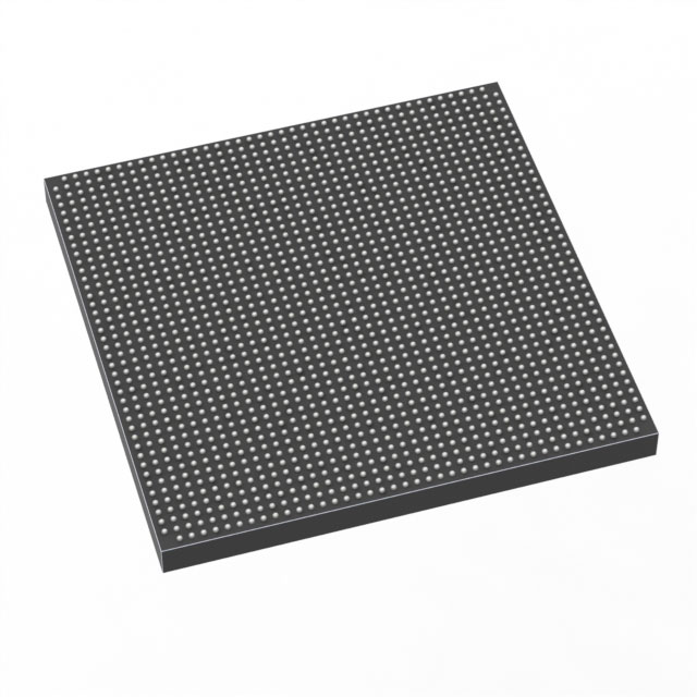
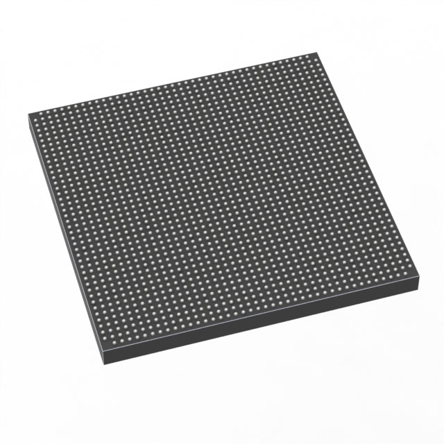
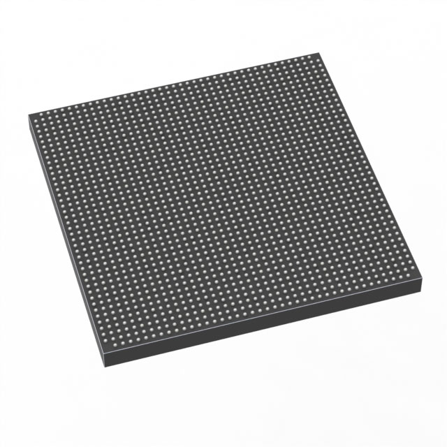
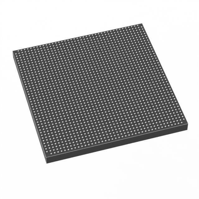
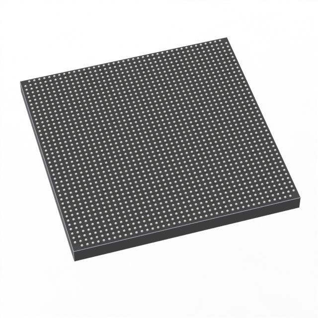
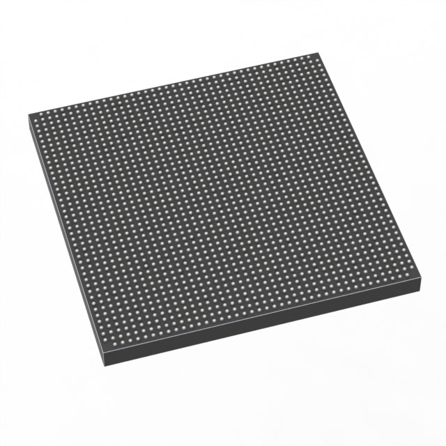
Stratix® 10 GX Field Programmable Gate Array (FPGA) IC 688 1650000 1760-BBGA, FCBGA |
|---|---|
| Quantity | 1,044 Available (as of October 8, 2026) |
| Product Category | Field Programmable Gate Array (FPGA) |
|---|---|
| Manufacturer | Intel |
| Manufacturing Status | Active |
| Manufacturer Standard Lead Time | 12 Weeks |
| Datasheet |
Specifications & Environmental
| Device Package | 1760-FBGA (42.5x42.5) | Grade | Extended | Operating Temperature | 0°C – 100°C | ||
|---|---|---|---|---|---|---|---|
| Package / Case | 1760-BBGA, FCBGA | Number of I/O | 688 | Voltage | 770 mV - 970 mV | ||
| Mounting Method | Surface Mount | RoHS Compliance | Unknown | REACH Compliance | REACH Unaffected | ||
| Moisture Sensitivity Level | 3 (168 Hours) | Number of LABs/CLBs | 206250 | Number of Logic Elements/Cells | 1650000 | ||
| Number of Gates | N/A | ECCN | N/A | HTS Code | N/A | ||
| Qualification | N/A | Total RAM Bits | 119537664 |
Overview of 1SG165HN2F43E2VG – Stratix® 10 GX FPGA, 1,650,000 logic elements (1760-FBGA)
The 1SG165HN2F43E2VG is an Intel Stratix® 10 GX field programmable gate array (FPGA) in a 1760-ball FCBGA package. It combines the Stratix 10 GX family architecture with high logic capacity and on-chip memory to address demanding, high-bandwidth processing applications.
Designed for advanced networking, compute acceleration, and high-speed I/O systems, this device leverages Intel’s Stratix 10 innovations—including the Hyperflex core architecture and heterogeneous 3D SiP transceiver technology—to deliver increased core performance and energy efficiency for complex FPGA designs.
Key Features
- Core architecture Built on the Intel Hyperflex core architecture and 14 nm tri-gate (FinFET) process; family-level improvements include up to 2× core performance versus previous-generation high-performance FPGAs.
- Logic capacity 1,650,000 logic elements suitable for large, complex designs and multi-function implementations.
- On-chip memory and DSP Total RAM: 119,537,664 bits; family features include M20K internal SRAM blocks and variable precision DSP blocks for high-throughput signal processing.
- I/O and transceivers 688 device I/Os; Stratix 10 family transceiver capabilities include up to 96 full-duplex transceiver channels and transceiver data rates up to 28.3 Gbps.
- Hard IP and interfaces Family-level integration includes PCI Express Gen3 x16 hard IP, hard 10G Ethernet FEC in transceiver channels, and hard memory controller/PHY supporting DDR4 rates (as described in Stratix 10 documentation).
- Package and mounting 1760-BBGA (FCBGA) package; supplier device package listed as 1760-FBGA (42.5 × 42.5 mm); surface-mount device.
- Power Core voltage supply range: 770 mV to 970 mV, enabling low-voltage core operation consistent with Stratix 10 family requirements.
- Temperature and grade Extended grade with an operating temperature range of 0 °C to 100 °C.
- Security and configuration Stratix 10 family features include secure device management, partial and dynamic reconfiguration, and SEU error detection and correction capabilities (family-level features described in the device overview).
- Compliance RoHS compliant.
Typical Applications
- High-performance networking and switch fabric Leverages abundant logic, large on-chip memory, and high-speed transceivers for packet processing, line cards, and backplane interfaces.
- Compute acceleration and data center Suitable for custom hardware acceleration workloads that require dense logic, DSP capability, and PCIe connectivity.
- Telecom and transport systems Supports high-throughput serial links and forward error correction in transceiver channels for transport and carrier-class equipment.
- High-speed memory interfaces Used where hard DDR4 controllers and PHY support at high data rates per pin are required (family-level memory support documented in the Stratix 10 overview).
Unique Advantages
- High logic density: 1,650,000 logic elements provide the capacity needed for large-scale, multi-function FPGA designs.
- Substantial on-chip RAM: 119,537,664 total RAM bits reduce dependence on external memory for many buffering and state-storage tasks.
- Extensive I/O and high-speed links: 688 I/Os and the family’s multi-gigabit transceiver architecture support complex interfacing and high-bandwidth data flows.
- Advanced packaging: 1760-ball FCBGA (42.5 × 42.5 mm) provides a compact, high-pin-count footprint for dense system integration.
- Low-voltage core operation: 770 mV–970 mV supply supports power-optimized core operation consistent with Stratix 10 power design.
- Extended operating range: 0 °C to 100 °C grade supports deployment in temperature environments aligned with the device grade.
Why Choose 1SG165HN2F43E2VG?
The 1SG165HN2F43E2VG delivers a combination of high logic capacity, significant on-chip memory, and extensive high-speed I/O in a compact 1760-FBGA package. It is well suited to designs that require substantial programmable fabric, integrated DSP resources, and advanced transceiver capability as described by the Stratix 10 GX family documentation.
Choose this device when your design priorities include dense logic resources, large internal memory, and robust I/O bandwidth in a surface-mount FCBGA form factor, with extended-grade operating temperature and RoHS compliance.
Request a quote or submit a product inquiry to discuss availability, pricing, and lead time for 1SG165HN2F43E2VG.





















Date Founded: 1968
Headquarters: Santa Clara, California, USA
Employees: 130,000+
Revenue: $54.23 Billion
Certifications and Memberships: ISO9001:2015, ISO14001:2015, ISO17025:2017, ISO27001:2022, ISO45001:2018, ISO50001:2018


