
1SG166HN3F43E3VG
| Part Description |
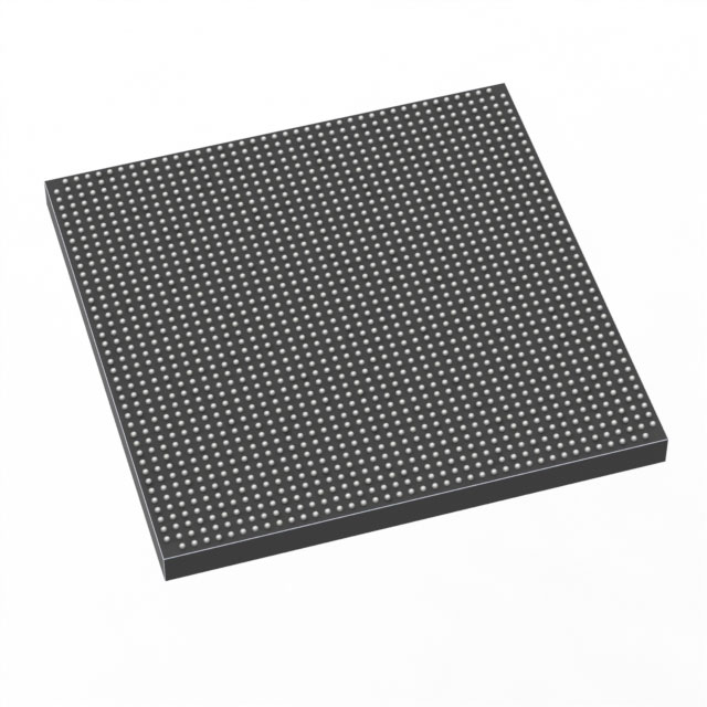
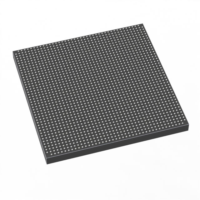
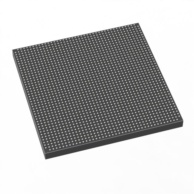
Stratix® 10 GX Field Programmable Gate Array (FPGA) IC 688 1660000 1760-BBGA, FCBGA |
|---|---|
| Quantity | 1 Available (as of October 8, 2026) |
| Product Category | Field Programmable Gate Array (FPGA) |
|---|---|
| Manufacturer | Intel |
| Manufacturing Status | Active |
| Manufacturer Standard Lead Time | 12 Weeks |
| Datasheet |
Specifications & Environmental
| Device Package | 1760-FBGA (42.5x42.5) | Grade | Extended | Operating Temperature | 0°C – 100°C | ||
|---|---|---|---|---|---|---|---|
| Package / Case | 1760-BBGA, FCBGA | Number of I/O | 688 | Voltage | 770 mV - 970 mV | ||
| Mounting Method | Surface Mount | RoHS Compliance | Unknown | REACH Compliance | REACH Unaffected | ||
| Moisture Sensitivity Level | 3 (168 Hours) | Number of LABs/CLBs | 207500 | Number of Logic Elements/Cells | 1660000 | ||
| Number of Gates | N/A | ECCN | N/A | HTS Code | N/A | ||
| Qualification | N/A | Total RAM Bits | 125829120 |
Overview of 1SG166HN3F43E3VG – Stratix® 10 GX FPGA, 1760-BBGA, Extended Grade
The 1SG166HN3F43E3VG is a Stratix® 10 GX field programmable gate array (FPGA) in a 1760-ball BGA (FCBGA) package, offered in an extended grade and intended for high-performance, board-mounted applications. It combines the Stratix 10 family’s Hyperflex core architecture and Intel 14 nm FinFET technology innovations with a high logic density and large embedded memory to address bandwidth- and compute-intensive designs.
This device delivers a substantial resource set—1,660,000 logic elements and 125,829,120 total RAM bits—along with 688 user I/Os, making it suitable for complex digital signal processing, high-density I/O aggregation, and designs requiring significant on-chip memory and logic capacity.
Key Features
- Core Logic 1,660,000 logic elements provide extensive programmable fabric for implementing large-scale logic, custom datapaths, and complex control systems.
- On‑Chip Memory 125,829,120 total RAM bits for intermediate buffering, large lookup tables, and memory-intensive algorithms.
- High‑Density I/O 688 I/O pins support wide parallel interfaces, high channel counts, or numerous peripheral connections on a single device.
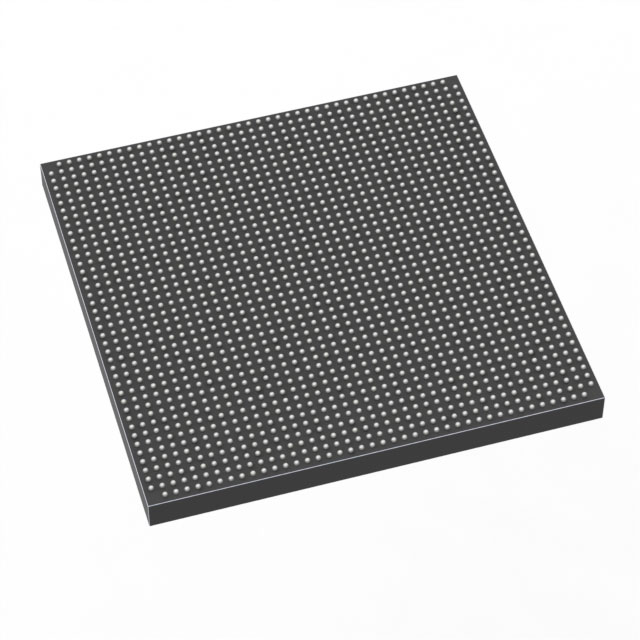
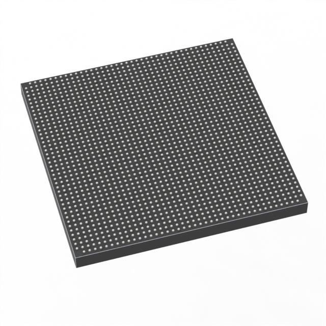
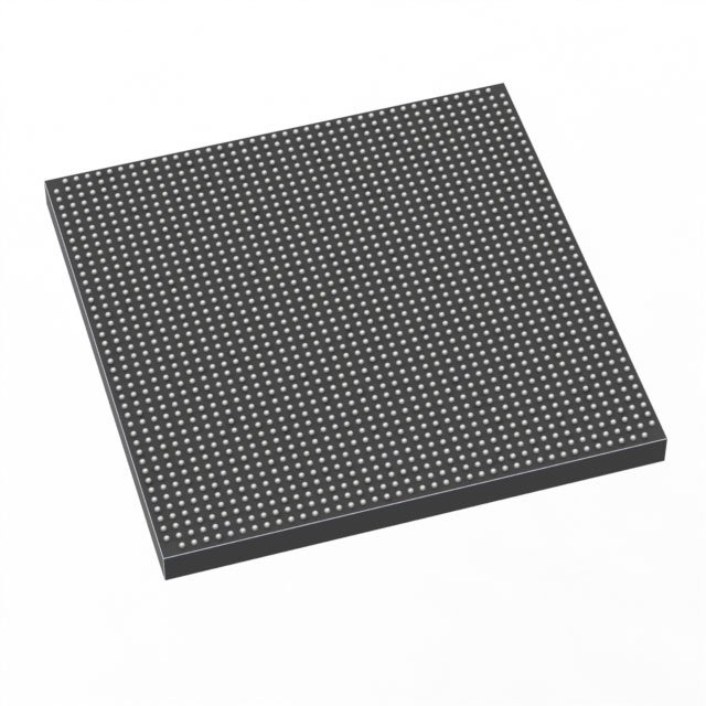
- Package and Mounting 1760-ball BGA (1760-FBGA, 42.5 × 42.5 mm) surface-mount package for high-pin-count board integration and reliable soldered mounting.
- Power Supply Supported core voltage range of 770 mV to 970 mV to match modern low-voltage FPGA power architectures.
- Operating Temperature Rated for operation from 0 °C to 100 °C in extended grade, suitable for many commercial and enterprise environments.
- Extended‑Grade Classification Offered in an extended grade to meet applications that require broader operational confidence than standard commercial grade.
Typical Applications
- High‑Performance Networking Implement packet processing, bandwidth aggregation, and protocol offload functions using the device’s high logic density and large on-chip memory.
- Data Center Acceleration Deploy as an FPGA accelerator for compute- and memory-intensive tasks where large logic capacity and substantial RAM bits reduce external memory dependence.
- Telecommunications and Backplane Systems Aggregate and route high-channel-count I/O for switch, router, or transport equipment leveraging the 688 available I/Os.
- Signal Processing and DSP Implement wide datapaths and buffering for advanced signal conditioning, filtering, and algorithmic processing that benefit from large embedded memory and logic.
Unique Advantages
- High logic capacity: 1,660,000 logic elements allow complex designs to be implemented on a single device, reducing system-level part count.
- Large embedded memory: 125,829,120 RAM bits provide ample on-chip storage for buffering and algorithm acceleration, minimizing external memory bandwidth requirements.
- Extensive I/O availability: 688 I/Os enable dense interfacing and high-channel-count connectivity without multiple devices.
- Robust packaging: 1760-ball FCBGA package (42.5 × 42.5 mm) supports high pin count and reliable surface-mount integration for complex boards.
- Optimized power range: Core voltage support from 770 mV to 970 mV aligns with modern low-voltage power systems to help manage overall board power design.
- Series innovation: Stratix 10 family advances such as the Hyperflex architecture and 14 nm FinFET process (as described in the Stratix 10 overview) bring improved core performance and power characteristics to designs based on this device.
Why Choose 1SG166HN3F43E3VG?
The 1SG166HN3F43E3VG positions itself for designs that demand large programmable logic, significant on-chip memory, and dense I/O in a single, board-mounted package. Its extended-grade rating, broad voltage support, and high-pin-count FCBGA package make it a strong candidate for enterprise, communications, and compute-accelerator applications where integration and scalability matter.
Engineers and system designers benefit from the Stratix 10 family’s architectural innovations combined with the specific device resources—logic elements, RAM bits, and I/O—providing a platform that scales for complex algorithms and high-bandwidth data paths while supporting established implementation flows.
Request a quote or submit an inquiry for part number 1SG166HN3F43E3VG to evaluate how this Stratix® 10 GX FPGA fits your next high-performance design.





















Date Founded: 1968
Headquarters: Santa Clara, California, USA
Employees: 130,000+
Revenue: $54.23 Billion
Certifications and Memberships: ISO9001:2015, ISO14001:2015, ISO17025:2017, ISO27001:2022, ISO45001:2018, ISO50001:2018


