
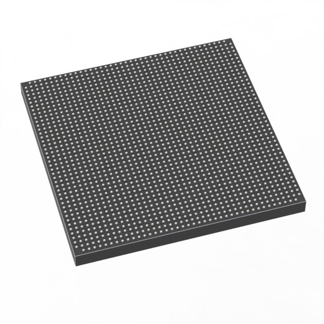
1SG166HN3F43I2LG
| Part Description |
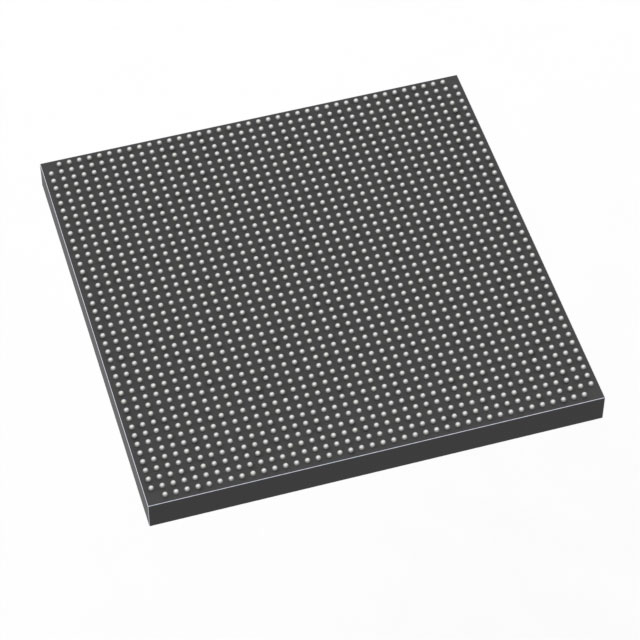
Stratix® 10 GX Field Programmable Gate Array (FPGA) IC 688 1660000 1760-BBGA, FCBGA |
|---|---|
| Quantity | 517 Available (as of October 7, 2026) |
| Product Category | Field Programmable Gate Array (FPGA) |
|---|---|
| Manufacturer | Intel |
| Manufacturing Status | Active |
| Manufacturer Standard Lead Time | 12 Weeks |
| Datasheet |
Specifications & Environmental
| Device Package | 1760-FBGA (42.5x42.5) | Grade | Industrial | Operating Temperature | -40°C – 100°C | ||
|---|---|---|---|---|---|---|---|
| Package / Case | 1760-BBGA, FCBGA | Number of I/O | 688 | Voltage | 820 mV - 880 mV | ||
| Mounting Method | Surface Mount | RoHS Compliance | Unknown | REACH Compliance | REACH Unaffected | ||
| Moisture Sensitivity Level | 3 (168 Hours) | Number of LABs/CLBs | 207500 | Number of Logic Elements/Cells | 1660000 | ||
| Number of Gates | N/A | ECCN | N/A | HTS Code | N/A | ||
| Qualification | N/A | Total RAM Bits | 125829120 |
Overview of 1SG166HN3F43I2LG – Stratix® 10 GX FPGA, 1,660,000 Logic Elements, 688 I/Os
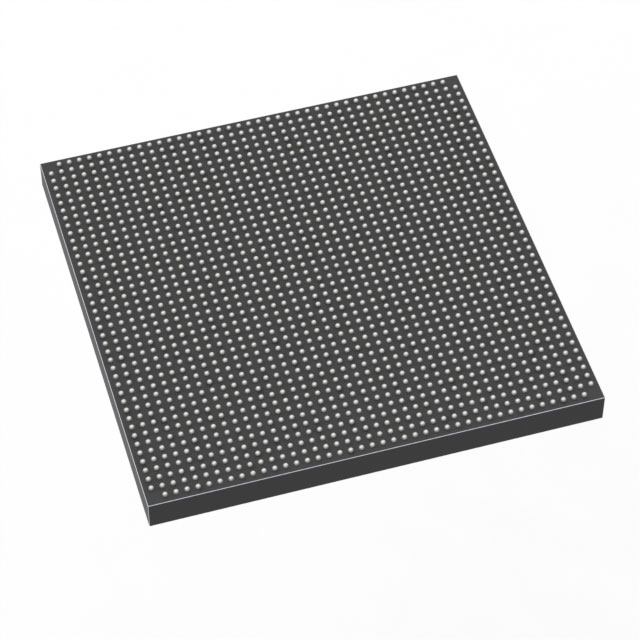
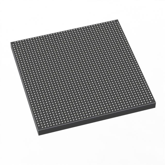
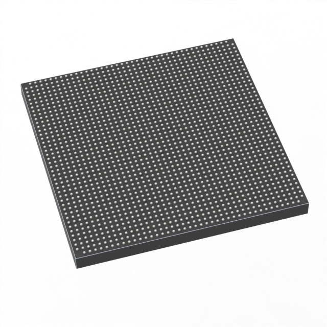
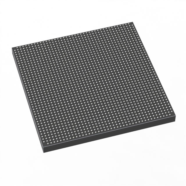
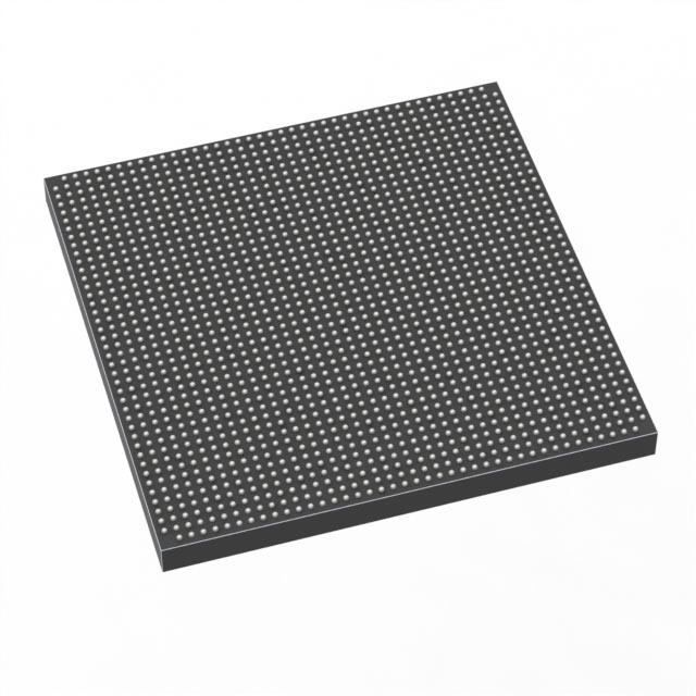
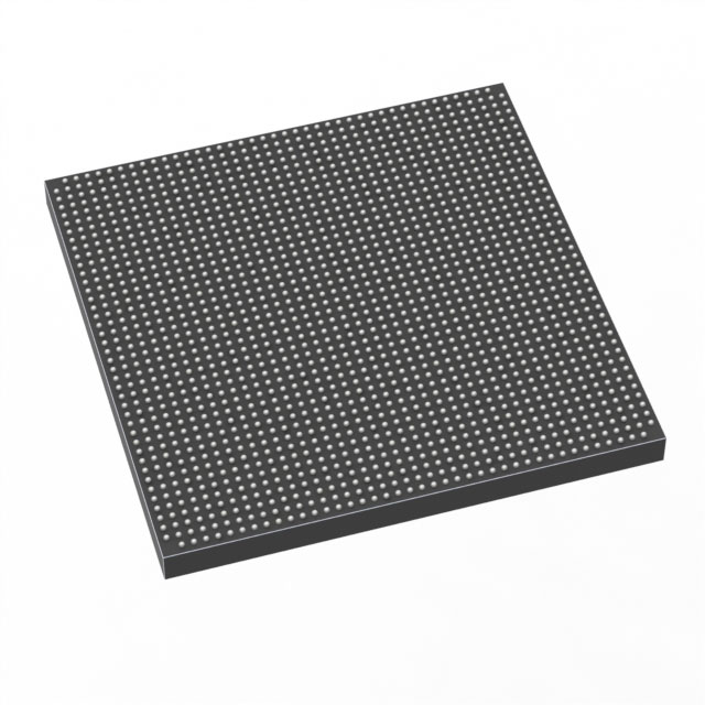
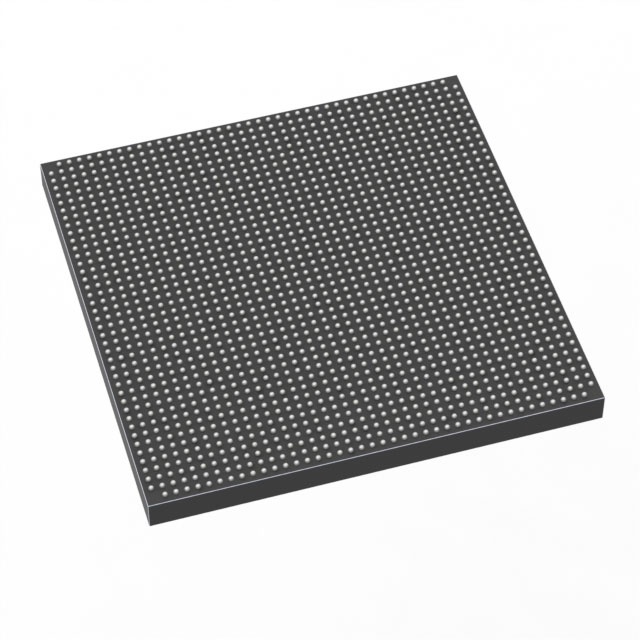
The Intel Stratix® 10 GX Field Programmable Gate Array (FPGA) 1SG166HN3F43I2LG is a high-capacity, industrial-grade FPGA in a 1760-BBGA FCBGA package. It combines a high logic element count with large on-chip RAM and extensive I/O to address demanding bandwidth and processing applications.
Built on the Stratix 10 family architecture, the device leverages the family’s Hyperflex core innovations and advanced process technologies to deliver increased core performance and integration for networking, communications, data center, and advanced embedded systems.
Key Features
- Logic Capacity 1,660,000 logic elements (LEs) to implement complex digital logic, large state machines, and deep pipeline designs.
- On-chip Memory 125,829,120 total RAM bits for buffering, packet memory, and accelerator local storage.
- I/O Density 688 I/Os to support wide external interfaces, parallel buses, and high-pin-count connectivity.
- Advanced Core Architecture Stratix 10 family Hyperflex core architecture (family-level feature) to enable higher core performance relative to previous-generation high-performance FPGAs.
- Transceiver and SiP Technology (Family) Family documentation lists heterogeneous 3D SiP transceiver tiles and high-speed transceivers capable of multi-gigabit rates for high-bandwidth interconnects.
- Power and Supply Core voltage range 820 mV to 880 mV for targeted power domains.
- Package and Mounting 1760-BBGA (1760-FBGA supplier package, 42.5 × 42.5 mm) surface-mount FCBGA for dense, board-level integration.
- Operating Range and Grade Industrial temperature range −40 °C to 100 °C; RoHS compliant.
Typical Applications
- High‑Performance Networking and Telecom Use the device to implement packet processing, PHY/PCS functions, and protocol offload with the device’s high logic density and large on-chip RAM.
- Data Center Acceleration Deploy as a hardware accelerator for compute and I/O intensive workloads where large logic fabric and substantial memory improve throughput and determinism.
- Backplane and Optical Interfaces Leverage the family’s high-speed transceiver architecture and the device’s abundant I/O for backplane, switch, and optical module interfacing.
- Advanced Embedded Systems Integrate complex control, signal processing, and custom interfaces in industrial and communications equipment using the device’s industrial temperature rating and high integration density.
Unique Advantages
- Massive Logic Resources: 1.66 million logic elements enable implementation of large, heterogeneous designs without partitioning across multiple FPGAs.
- Large On‑Chip Memory: 125.8 Mb of RAM bits provides local buffering and storage to reduce external memory bandwidth and simplify timing closure.
- High I/O Count: 688 I/Os let designers route wide data buses, multiple interfaces, and dense peripheral connectivity directly to the FPGA.
- Industrial‑Temperature Operation: Rated for −40 °C to 100 °C to meet industrial environment requirements and extended operating ranges.
- Compact, High‑Density Package: 1760-BBGA FCBGA package (42.5 × 42.5 mm supplier package) supports high-pin-count designs in a single-package solution.
- RoHS Compliance: Meets regulatory requirements for environmental and material compliance.
Why Choose 1SG166HN3F43I2LG?
The 1SG166HN3F43I2LG provides a balanced combination of large logic capacity, significant on-chip RAM, and extensive I/O in an industrial-grade Stratix 10 GX FPGA package. It is positioned for designers who need to consolidate complex processing, high-throughput I/O, and substantial buffering into a single, surface-mount FPGA solution.
For teams developing networking, data center, communications, and advanced embedded applications, this device offers scalability and integration that reduce system complexity and board-level component count while supporting demanding performance and environmental requirements.
Request a quote or submit a product inquiry to evaluate 1SG166HN3F43I2LG for your next high‑performance FPGA design.





















Date Founded: 1968
Headquarters: Santa Clara, California, USA
Employees: 130,000+
Revenue: $54.23 Billion
Certifications and Memberships: ISO9001:2015, ISO14001:2015, ISO17025:2017, ISO27001:2022, ISO45001:2018, ISO50001:2018


