
1SG211HN3F43E2LG
| Part Description |
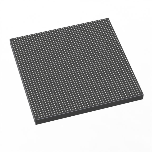
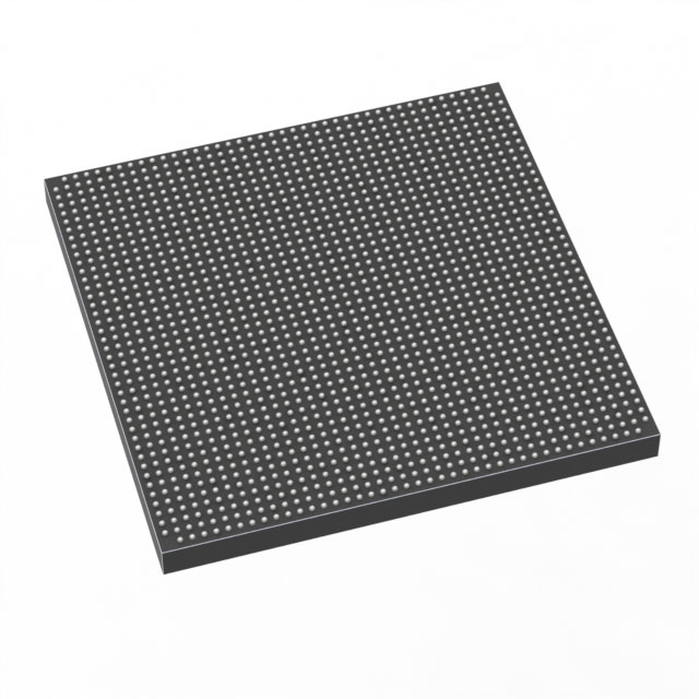
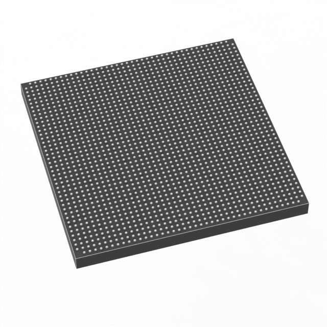
Stratix® 10 GX Field Programmable Gate Array (FPGA) IC 688 2110000 1760-BBGA, FCBGA |
|---|---|
| Quantity | 140 Available (as of October 8, 2026) |
| Product Category | Field Programmable Gate Array (FPGA) |
|---|---|
| Manufacturer | Intel |
| Manufacturing Status | Active |
| Manufacturer Standard Lead Time | 12 Weeks |
| Datasheet |
Specifications & Environmental
| Device Package | 1760-FBGA (42.5x42.5) | Grade | Extended | Operating Temperature | 0°C – 100°C | ||
|---|---|---|---|---|---|---|---|
| Package / Case | 1760-BBGA, FCBGA | Number of I/O | 688 | Voltage | 820 mV - 880 mV | ||
| Mounting Method | Surface Mount | RoHS Compliance | Unknown | REACH Compliance | REACH Unaffected | ||
| Moisture Sensitivity Level | 3 (168 Hours) | Number of LABs/CLBs | 263750 | Number of Logic Elements/Cells | 2110000 | ||
| Number of Gates | N/A | ECCN | N/A | HTS Code | N/A | ||
| Qualification | N/A | Total RAM Bits | 140509184 |
Overview of 1SG211HN3F43E2LG – Stratix® 10 GX FPGA, 1760‑BBGA (FCBGA)
The 1SG211HN3F43E2LG is an Intel Stratix® 10 GX field‑programmable gate array in a 1760‑BBGA (FCBGA) package. It delivers a high density FPGA fabric combined with the Stratix 10 family innovations such as the Intel Hyperflex™ core architecture and Intel 14 nm tri‑gate (FinFET) process.
Designed for high‑performance networking, data center and signal‑processing designs, this device offers a combination of large logic capacity, extensive on‑chip RAM and high I/O count for compute‑ and bandwidth‑intensive applications while operating over an extended temperature range.
Key Features
- Core & architecture Stratix 10 family innovations are included in this GX device family, including the Intel Hyperflex core architecture and 14 nm tri‑gate (FinFET) technology to enable increased core performance.
- Logic capacity 2,110,000 logic elements provide very large programmable logic resources for complex FPGA implementations.
- On‑chip memory 140,509,184 total RAM bits of internal memory for buffering, scratch memory and storage of large datasets inside the fabric.
- I/O and connectivity 688 user I/Os support high‑density external interfacing and system integration.
- Package and mounting 1760‑BBGA (FCBGA) supplier package 1760‑FBGA with a 42.5 × 42.5 mm footprint, surface‑mountable for high‑density board designs.
- Power Core supply operating range specified at 820 mV to 880 mV to match advanced low‑voltage FPGA power domains.
- Temperature & grade Extended grade device rated for 0 °C to 100 °C operating temperature.
- Compliance RoHS compliant for global lead‑free process requirements.
- Family‑level connectivity and IP The Stratix 10 GX family includes high‑speed transceiver and IP capabilities (family documentation cites heterogeneous 3D SiP transceiver tiles and transceiver data rates up to 28.3 Gbps), enabling advanced serial connectivity options when used in systems targeting those features.
Typical Applications
- High‑performance networking Use for line cards, switches and routers where large logic capacity and dense I/O enable complex packet processing and high port counts.
- Data center acceleration Suitable for FPGA‑based acceleration tasks that require significant on‑chip RAM and logic for custom compute kernels and buffering.
- High‑speed serial interfaces Applicable to backplane and module designs that leverage the Stratix 10 GX family’s transceiver capabilities and high I/O density.
- Signal processing and DSP Deploy in systems that need substantial logic resources and internal memory for real‑time processing, filtering and aggregation.
Unique Advantages
- High logic density: 2,110,000 logic elements provide headroom for large, complex designs without partitioning across multiple devices.
- Substantial on‑chip RAM: 140,509,184 total RAM bits reduce dependency on external memory for many buffering and real‑time data tasks.
- Large I/O capability: 688 I/Os enable high port counts and flexible board‑level interfacing for complex systems.
- Compact, manufacturable package: 1760‑BBGA (42.5 × 42.5 mm) FCBGA package supports surface‑mount assembly in dense PCB layouts.
- Low‑voltage core operation: Specified 820 mV–880 mV core supply aligns with modern low‑power FPGA design practices.
- Extended operating grade: Rated for 0 °C to 100 °C, enabling deployment in a wide range of commercial and enterprise environments.
Why Choose 1SG211HN3F43E2LG?
1SG211HN3F43E2LG positions itself as a high‑density Stratix 10 GX FPGA option for developers who need a large programmable fabric, abundant on‑chip RAM, and substantial I/O capacity in a single package. Its specification set supports complex networking, acceleration and signal processing applications that require both logic density and memory bandwidth.
As a member of the Stratix 10 family, it provides a scalable path within a product line that documents advanced core architecture and connectivity innovations, making it suitable for teams designing high‑performance systems that leverage the family’s capabilities.
Request a quote or submit an inquiry to discuss pricing, availability and delivery for part number 1SG211HN3F43E2LG.





















Date Founded: 1968
Headquarters: Santa Clara, California, USA
Employees: 130,000+
Revenue: $54.23 Billion
Certifications and Memberships: ISO9001:2015, ISO14001:2015, ISO17025:2017, ISO27001:2022, ISO45001:2018, ISO50001:2018


