
1SG211HN3F43E2VG
| Part Description |
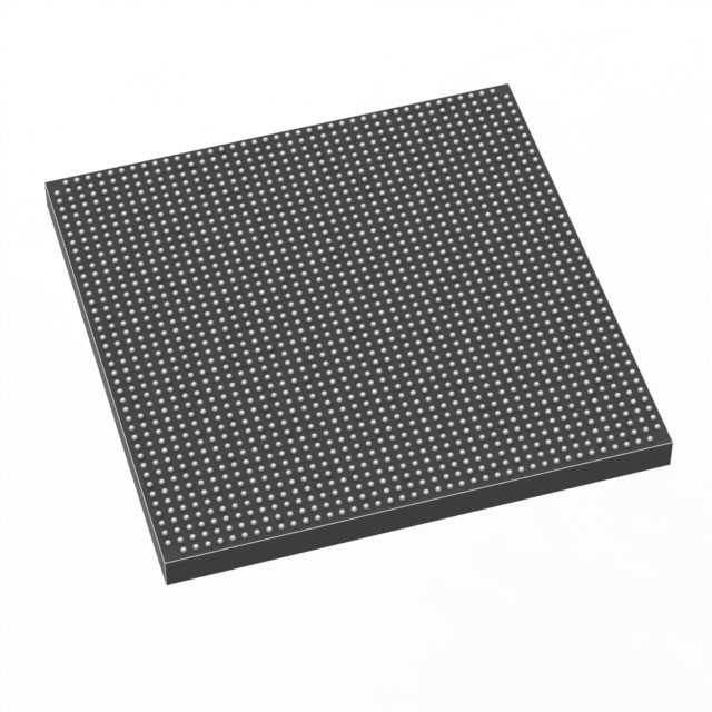
Stratix® 10 GX Field Programmable Gate Array (FPGA) IC 688 2110000 1760-BBGA, FCBGA |
|---|---|
| Quantity | 70 Available (as of June 9, 2026) |

| Product Category | Field Programmable Gate Array (FPGA) |
|---|---|
| Manufacturer | Intel |
| Manufacturing Status | Active |
| Manufacturer Standard Lead Time | 12 Weeks |
| Datasheet |
Specifications & Environmental
| Device Package | 1760-FBGA (42.5x42.5) | Grade | Extended | Operating Temperature | 0°C – 100°C | ||
|---|---|---|---|---|---|---|---|
| Package / Case | 1760-BBGA, FCBGA | Number of I/O | 688 | Voltage | 770 mV - 970 mV | ||
| Mounting Method | Surface Mount | RoHS Compliance | Unknown | REACH Compliance | REACH Unaffected | ||
| Moisture Sensitivity Level | 3 (168 Hours) | Number of LABs/CLBs | 263750 | Number of Logic Elements/Cells | 2110000 | ||
| Number of Gates | N/A | ECCN | N/A | HTS Code | N/A | ||
| Qualification | N/A | Total RAM Bits | 140509184 |
Overview of 1SG211HN3F43E2VG – Stratix® 10 GX Field Programmable Gate Array (FPGA) IC 688 2110000 1760-BBGA, FCBGA
The Intel Stratix® 10 GX FPGA 1SG211HN3F43E2VG is a high-density, high-performance field programmable gate array optimized for advanced bandwidth and compute applications. Built on the Stratix 10 family architecture, it pairs the Intel Hyperflex™ core architecture and Intel 14 nm process innovations to address demanding communications, compute acceleration, and high-throughput signal processing use cases.
This device provides a combination of large logic capacity, extensive on-chip RAM, and broad I/O plus package options to enable complex, high-performance system designs that require substantial programmable fabric and robust I/O support.
Key Features
- Core & architecture All-new Intel Hyperflex™ core architecture and Intel 14 nm tri-gate (FinFET) process technology, providing family-level performance and power advantages described for Stratix 10 devices.
- Logic capacity Approximately 2,110,000 logic elements to implement large, complex programmable designs.
- On-chip memory Total RAM capacity of 140,509,184 bits, supported by Stratix 10 internal SRAM block structures (M20K memory blocks as part of the family architecture).
- I/O and package 688 I/O pins with a 1760-BBGA FCBGA package (supplier device package: 1760-FBGA, 42.5 × 42.5 mm) designed for surface-mount assembly.
- High-speed transceivers and interfaces Series-level transceiver technology and interface IP in the Stratix 10 family support high data-rate serial links and protocol hard IP (family overview includes up to 28.3 Gbps transceiver data rates and hard PCI Express and Ethernet IP options).
- Power supply and operating range Core voltage supply range of 770 mV to 970 mV and an operating temperature range of 0 °C to 100 °C; device grade specified as Extended.
- Advanced DSP and compute Family-level variable-precision DSP blocks and architecture innovations provide high compute capability for signal processing workloads.
Typical Applications
- High-performance networking Leverage the device's high logic density, extensive I/O and Stratix 10 transceiver technology to implement line-rate packet processing, switching and protocol offload functions.
- Data center acceleration Large logic capacity and substantial on-chip RAM make this FPGA suitable for custom acceleration engines, data-plane processing, and compute offload tasks.
- High-bandwidth interconnects Use the device's family-level high-speed transceiver capability and abundant I/O to build high-throughput chip-to-chip and backplane interfaces.
- Signal processing and DSP High logic and memory resources combined with Stratix 10 DSP blocks support complex fixed- and floating-point signal processing chains.
Unique Advantages
- High logic density: With approximately 2,110,000 logic elements, the device supports large, integrated designs without partitioning across multiple FPGAs.
- Substantial on-chip memory: 140,509,184 bits of RAM enable deep buffering, large lookup tables, and stateful processing directly in the FPGA fabric.
- Robust I/O and packaging: 688 I/O pins in a 1760-BBGA (1760-FBGA package) provide extensive external connectivity while supporting surface-mount assembly.
- Series-level high-speed capabilities: Stratix 10 family transceiver and protocol IP options (including PCIe and Ethernet hard IP described in the family overview) help accelerate implementation of complex interfaces.
- Power and process advantages: Intel 14 nm FinFET process and Hyperflex architecture (family features) contribute to improved performance-per-watt for high-throughput designs.
- Extended-grade operation: Specified operating range of 0 °C to 100 °C and extended grade classification align with demanding commercial and data center environments.
Why Choose 1SG211HN3F43E2VG?
The 1SG211HN3F43E2VG Stratix 10 GX FPGA delivers a balance of very high logic capacity, significant on-chip memory, and extensive I/O in a 1760-BBGA package. It is positioned for engineers building advanced communications, compute acceleration, and signal processing systems that require large programmable fabric combined with high-speed interface capability described for the Stratix 10 family.
Choosing this device provides a path to scalable designs that leverage family-level innovations—Hyperflex architecture, advanced process technology, and high-speed interface IP—backed by Intel's Stratix 10 device ecosystem and documentation.
Request a quote or submit an inquiry to start evaluating 1SG211HN3F43E2VG for your next high-performance FPGA design project.


Date Founded: 1968
Headquarters: Santa Clara, California, USA
Employees: 130,000+
Revenue: $54.23 Billion
Certifications and Memberships: ISO9001:2015, ISO14001:2015, ISO17025:2017, ISO27001:2022, ISO45001:2018, ISO50001:2018


