
1SG211HN3F43E3VG
| Part Description |
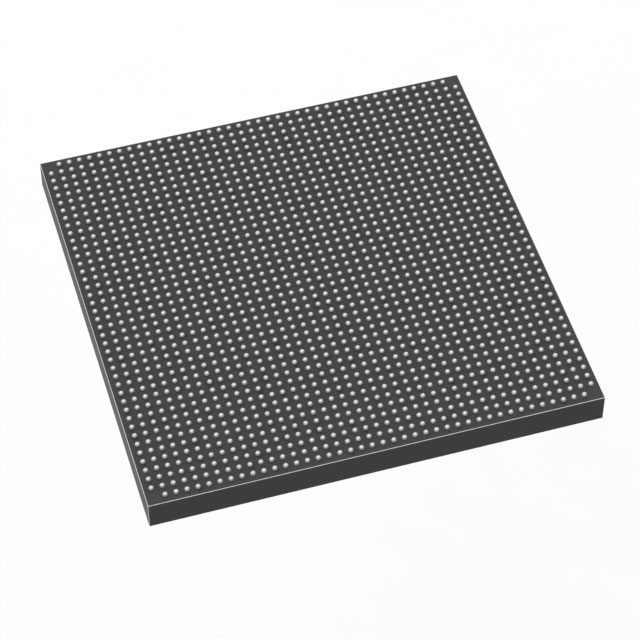
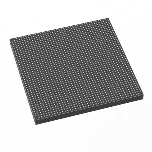
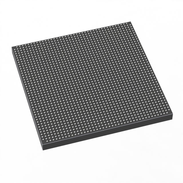
Stratix® 10 GX Field Programmable Gate Array (FPGA) IC 688 2110000 1760-BBGA, FCBGA |
|---|---|
| Quantity | 285 Available (as of October 7, 2026) |
| Product Category | Field Programmable Gate Array (FPGA) |
|---|---|
| Manufacturer | Intel |
| Manufacturing Status | Active |
| Manufacturer Standard Lead Time | 12 Weeks |
| Datasheet |
Specifications & Environmental
| Device Package | 1760-FBGA (42.5x42.5) | Grade | Extended | Operating Temperature | 0°C – 100°C | ||
|---|---|---|---|---|---|---|---|
| Package / Case | 1760-BBGA, FCBGA | Number of I/O | 688 | Voltage | 770 mV - 970 mV | ||
| Mounting Method | Surface Mount | RoHS Compliance | Unknown | REACH Compliance | REACH Unaffected | ||
| Moisture Sensitivity Level | 3 (168 Hours) | Number of LABs/CLBs | 263750 | Number of Logic Elements/Cells | 2110000 | ||
| Number of Gates | N/A | ECCN | N/A | HTS Code | N/A | ||
| Qualification | N/A | Total RAM Bits | 140509184 |
Overview of 1SG211HN3F43E3VG – Stratix® 10 GX FPGA, 1760‑BBGA FCBGA
The 1SG211HN3F43E3VG is a Stratix® 10 GX field programmable gate array (FPGA) in a 1760‑BBGA (FCBGA) package, designed for high-performance, bandwidth‑intensive designs. Built on the Intel Stratix 10 family, this device leverages the Hyperflex core architecture and Intel 14 nm tri‑gate process innovations to deliver scalable core performance and advanced system integration.
With 2,110,000 logic elements, extensive on‑chip RAM, and high I/O density, this FPGA targets applications that require large logic capacity, significant memory resources, and plentiful I/O while operating within a core supply range of 770 mV to 970 mV and an ambient range of 0 °C to 100 °C.
Key Features
- Core architecture Intel Hyperflex™ core architecture and 14 nm tri‑gate (FinFET) technology deliver the family‑level performance and efficiency characteristics described in the Stratix 10 GX device overview.
- Logic capacity 2,110,000 logic elements provide large programmable resources for complex designs and high‑density implementation.
- On‑chip memory 140,509,184 total RAM bits (internal SRAM) offer substantial embedded memory for buffering, packet processing, and intermediate data storage.
- I/O and connectivity 688 I/O pins deliver high external connectivity; family documentation highlights heterogeneous transceiver tiles and multi‑Gbps transceiver support for high‑bandwidth interconnects.
- DSP and compute Stratix 10 family variable precision DSP blocks and hard IP enable heavy signal processing workloads; family materials document substantial compute throughput and efficient DSP performance.
- Hard IP and interfaces Family‑level features include hard PCI Express Gen3 IP, hard memory controllers supporting DDR4 rates, and advanced transceiver PCS/PMA capabilities for common high‑speed protocols.
- Power and supply Device core supply range: 770 mV to 970 mV, enabling operation within the specified voltage window for the device.
- Package and mounting Surface mount, 1760‑BBGA (supplier package: 1760‑FBGA, 42.5 mm × 42.5 mm) for system integration where high I/O density and thermal considerations are required.
- Operating and grade Extended grade device rated for an operating temperature range of 0 °C to 100 °C and RoHS compliant.
Typical Applications
- High‑performance networking — Large logic capacity, extensive on‑chip RAM and high I/O count support packet processing, switching, and custom forwarding engines.
- Data center acceleration — Dense programmable logic and DSP resources enable compute acceleration, encryption, and custom offload functions.
- Telecom and backplane systems — Family transceiver capabilities and abundant I/O make the device suitable for high‑speed backplane and line‑card designs.
- Signal processing — Substantial embedded memory and DSP resources support real‑time filtering, encoding/decoding, and complex arithmetic pipelines.
Unique Advantages
- Large programmable fabric: 2,110,000 logic elements provide headroom for complex, high‑density implementations without immediate partitioning to external logic.
- Significant on‑chip memory: 140,509,184 total RAM bits reduce dependency on external memory for many buffering and working‑set needs.
- High I/O density: 688 I/Os enable broad peripheral connectivity and high‑pin‑count system interfaces.
- Advanced family features: Stratix 10 family innovations (Hyperflex core, 14 nm tri‑gate, heterogeneous SiP/transceiver capabilities) support higher core performance and system integration options.
- Robust packaging for dense systems: 1760‑BBGA FCBGA (42.5 mm × 42.5 mm) provides a compact, surface‑mount footprint suitable for advanced system boards.
- Compliance and grade: Extended grade and RoHS compliance make the device suitable for demanding commercial and industrial environments within the specified temperature range.
Why Choose 1SG211HN3F43E3VG?
The 1SG211HN3F43E3VG brings a high‑capacity Stratix 10 GX FPGA into a 1760‑BBGA package, combining 2,110,000 logic elements with extensive on‑chip RAM and a 688‑pin I/O interface. Its specification aligns with applications that require substantial programmable resources, high I/O density, and the integration advantages of the Stratix 10 family architecture.
Engineers designing networking equipment, data center accelerators, telecom line cards, or advanced signal processing systems will find the device’s logic, memory, and connectivity attributes suitable for scalable, high‑performance implementations, while the extended grade and RoHS compliance support reliable deployment within the stated operating range.
Request a quote or contact our sales team to discuss availability, pricing, and technical support for 1SG211HN3F43E3VG.





















Date Founded: 1968
Headquarters: Santa Clara, California, USA
Employees: 130,000+
Revenue: $54.23 Billion
Certifications and Memberships: ISO9001:2015, ISO14001:2015, ISO17025:2017, ISO27001:2022, ISO45001:2018, ISO50001:2018


