
1SG250HH1F55E1VG
| Part Description |
Stratix® 10 GX Field Programmable Gate Array (FPGA) IC 1160 2500000 2912-BBGA, FCBGA |
|---|---|
| Quantity | 265 Available (as of June 15, 2026) |

| Product Category | Field Programmable Gate Array (FPGA) |
|---|---|
| Manufacturer | Intel |
| Manufacturing Status | Active |
| Manufacturer Standard Lead Time | 12 Weeks |
| Datasheet |
Specifications & Environmental
| Device Package | 2912-FBGA, FC (55x55) | Grade | Extended | Operating Temperature | 0°C – 100°C | ||
|---|---|---|---|---|---|---|---|
| Package / Case | 2912-BBGA, FCBGA | Number of I/O | 1160 | Voltage | 770 mV - 970 mV | ||
| Mounting Method | Surface Mount | RoHS Compliance | Unknown | REACH Compliance | REACH Unaffected | ||
| Moisture Sensitivity Level | 3 (168 Hours) | Number of LABs/CLBs | 312500 | Number of Logic Elements/Cells | 2500000 | ||
| Number of Gates | N/A | ECCN | N/A | HTS Code | N/A | ||
| Qualification | N/A | Total RAM Bits | 204472320 |
Overview of 1SG250HH1F55E1VG – Stratix® 10 GX FPGA, 2,500,000 logic elements, 1,160 I/Os
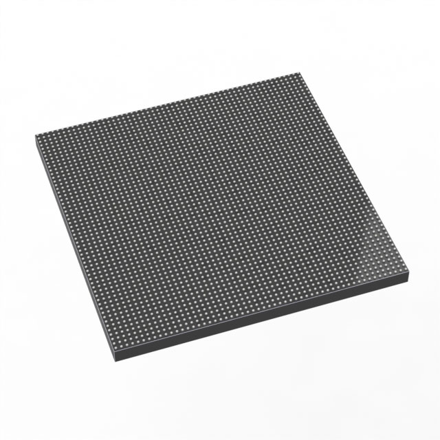
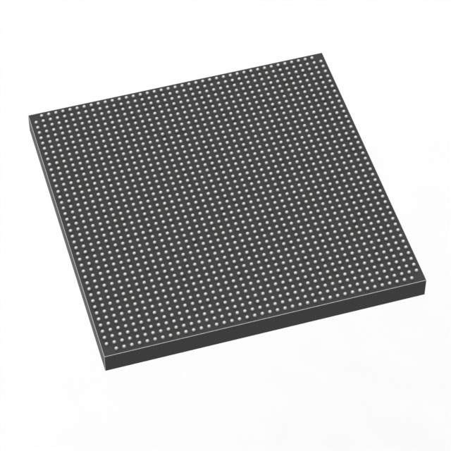
The 1SG250HH1F55E1VG is an Intel Stratix® 10 GX Field Programmable Gate Array (FPGA) delivered in a 2912-BBGA (FCBGA, 55×55) surface-mount package. This device provides 2,500,000 logic elements and 204,472,320 bits of on-chip RAM to support high-capacity, high-throughput hardware designs.
Built on Stratix 10 family innovations, the device leverages the Intel Hyperflex core architecture and Intel 14 nm tri‑gate (FinFET) process technology to address advanced applications that demand high logic density, substantial on-chip memory, and large I/O counts. It is offered in an Extended grade and is RoHS compliant.
Key Features
- Logic Capacity 2,500,000 logic elements suitable for large FPGA designs and complex processing pipelines.
- On‑chip Memory 204,472,320 total RAM bits to support large buffering, frame storage, and embedded memory requirements.
- I/O Density 1,160 user I/Os to accommodate wide parallel interfaces, large memory buses, or multiple high-speed interfaces.
- Core Architecture Intel Hyperflex core architecture and Intel 14 nm tri‑gate (FinFET) technology, as documented for the Stratix 10 family.
- High‑speed Fabric and IP Family-level features include heterogeneous 3D SiP transceiver tiles, hard PCI Express Gen3 IP options, and hard Ethernet/FEC features (as described in Stratix 10 GX/SX device documentation).
- DSP and Compute Family documents describe variable-precision DSP blocks and high compute capability for signal-processing workloads.
- Power and Clocking Device supports advanced clocking and PLL features described in the Stratix 10 family documentation; nominal core supply range is 770 mV to 970 mV.
- Package and Mounting 2912‑BBGA (FCBGA, 55×55) package, surface mount, suitable for compact, high-density board layouts.
- Operating Range and Grade Extended grade with an operating temperature range of 0 °C to 100 °C; RoHS compliant.
Typical Applications
- High‑performance networking and switching: Large logic capacity, extensive I/O, and family-level high-speed transceiver features make the device suitable for line cards, packet processing, and backplane interfaces.
- Data center acceleration: Dense logic resources and substantial on-chip RAM support custom accelerator functions and large buffering for compute and storage offload.
- Advanced signal processing: On-chip memory and family-level DSP block capabilities enable implementation of complex digital signal processing chains for communications and test equipment.
- Storage and interconnect PHYs: Hard IP and high I/O count support implementation of protocol bridges, memory interfaces, and high-bandwidth interconnects.
Unique Advantages
- Large, scalable logic capacity: 2,500,000 logic elements provide headroom for complex, multi‑function hardware designs without immediate migration.
- Substantial embedded memory: Over 204 million bits of on‑chip RAM reduces reliance on external memory for buffering and accelerates data‑path performance.
- High I/O count: 1,160 I/Os enable broad connectivity options for wide buses, parallel interfaces, and multi‑lane designs.
- Advanced family architecture: Intel Hyperflex core architecture and 14 nm FinFET process technology (Stratix 10 family) support higher core efficiency and performance characteristics described for the family.
- Package density: 2912‑BBGA FCBGA (55×55) package provides a compact form factor for high‑pin‑count implementations.
- Extended grade and compliance: Extended operating temperature range (0 °C to 100 °C) and RoHS compliance for a wide set of deployment environments.
Why Choose 1SG250HH1F55E1VG?
The 1SG250HH1F55E1VG positions itself where high logic density, large on‑chip memory, and extensive I/O are required. It brings Stratix 10 family architecture advantages—such as the Intel Hyperflex core and 14 nm tri‑gate process—into designs that require substantial programmable resources and a dense package footprint.
This device is well suited to teams designing high‑bandwidth networking, compute acceleration, or advanced signal processing systems that need scalable logic, significant embedded RAM, and a high I/O count. Its Extended temperature grade and RoHS compliance help ensure suitability across a range of deployment scenarios.
If you need pricing, availability, or technical procurement details, request a quote or submit an inquiry to receive a formal quotation and assistance with your design requirements.


Date Founded: 1968
Headquarters: Santa Clara, California, USA
Employees: 130,000+
Revenue: $54.23 Billion
Certifications and Memberships: ISO9001:2015, ISO14001:2015, ISO17025:2017, ISO27001:2022, ISO45001:2018, ISO50001:2018


