
1SG250HH1F55I2VG
| Part Description |
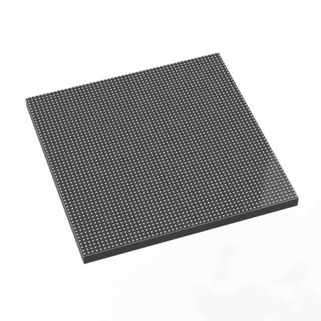
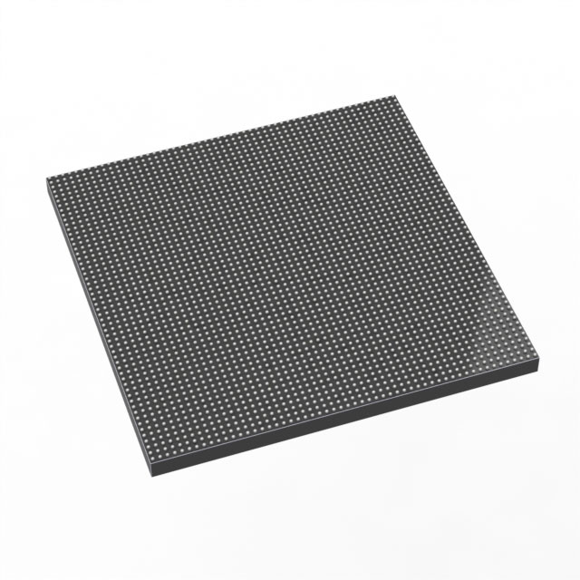
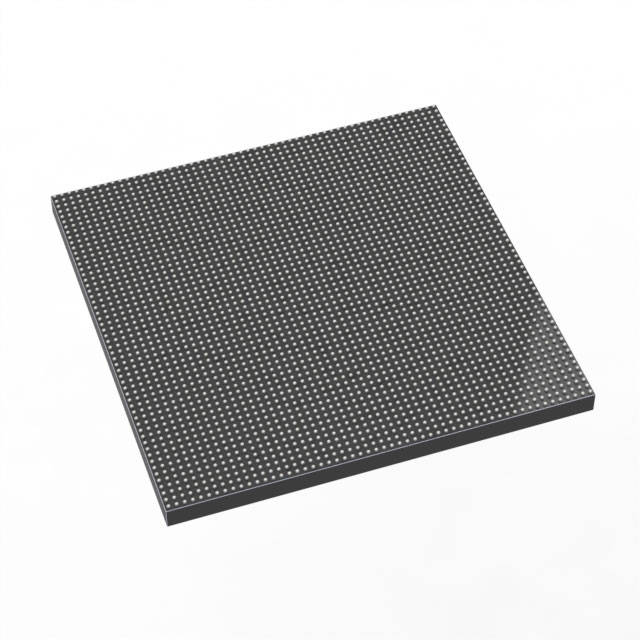
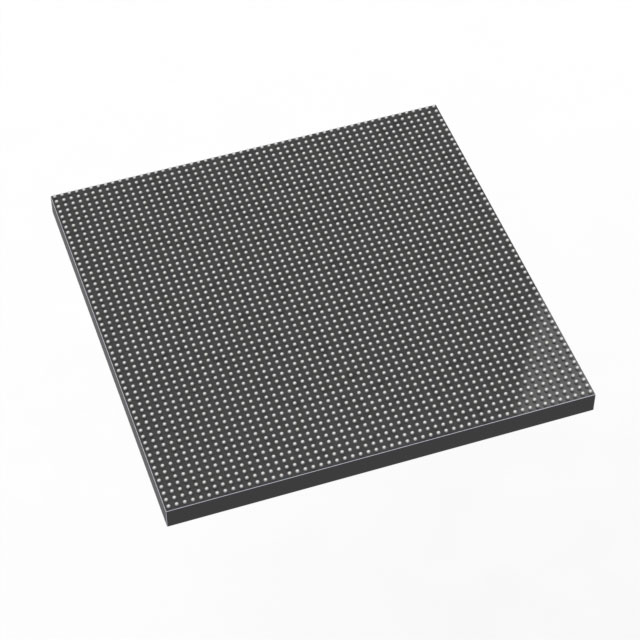
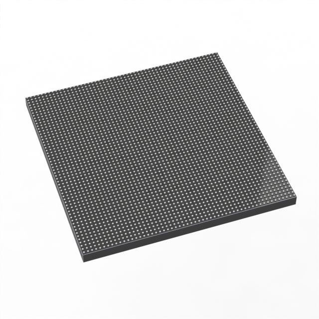
Stratix® 10 GX Field Programmable Gate Array (FPGA) IC 1160 2500000 2912-BBGA, FCBGA |
|---|---|
| Quantity | 1,032 Available (as of October 8, 2026) |
| Product Category | Field Programmable Gate Array (FPGA) |
|---|---|
| Manufacturer | Intel |
| Manufacturing Status | Active |
| Manufacturer Standard Lead Time | 12 Weeks |
| Datasheet |
Specifications & Environmental
| Device Package | 2912-FBGA, FC (55x55) | Grade | Industrial | Operating Temperature | -40°C – 100°C | ||
|---|---|---|---|---|---|---|---|
| Package / Case | 2912-BBGA, FCBGA | Number of I/O | 1160 | Voltage | 770 mV - 970 mV | ||
| Mounting Method | Surface Mount | RoHS Compliance | Unknown | REACH Compliance | REACH Unaffected | ||
| Moisture Sensitivity Level | 3 (168 Hours) | Number of LABs/CLBs | 312500 | Number of Logic Elements/Cells | 2500000 | ||
| Number of Gates | N/A | ECCN | N/A | HTS Code | N/A | ||
| Qualification | N/A | Total RAM Bits | 204472320 |
Overview of 1SG250HH1F55I2VG – Stratix® 10 GX Field Programmable Gate Array (FPGA)
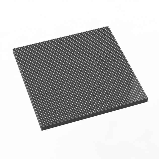
The 1SG250HH1F55I2VG is an Intel Stratix® 10 GX FPGA offered in a 2912‑FBGA surface‑mount package. It delivers a high‑density programmable fabric with 2,500,000 logic elements and a large embedded RAM resource for advanced, bandwidth‑intensive digital designs.
Built on the Stratix 10 family architecture, the device targets high‑performance applications that require advanced core architecture, significant on‑chip memory, high I/O counts and wide operating temperature range for industrial deployments.
Key Features
- Logic Density 2,500,000 logic elements (LEs) to implement large, complex FPGA designs and deep custom logic integration.
- On‑Chip Memory 204,472,320 total RAM bits of embedded SRAM to support buffering, large lookup tables and partitioned memory architectures.
- I/O Capability 1,160 device I/O pins, enabling wide parallel interfaces and dense connectivity to external components and daughtercards.
- Core Architecture Stratix 10 family innovations including the Intel Hyperflex™ core architecture and Intel 14 nm tri‑gate (FinFET) technology as described in the device overview.
- Power Supply Core voltage operating range from 770 mV to 970 mV to match modern low‑voltage power architectures.
- Package and Mounting 2912‑FBGA (55 × 55 mm) FCBGA package, surface‑mount for high‑density board designs.
- Operating Temperature Industrial temperature grade: −40 °C to +100 °C for reliable operation in demanding environments.
- Standards Compliance RoHS compliant, meeting common environmental regulatory requirements for lead‑free assembly.
Typical Applications
- Telecommunications & Networking Implement high‑bandwidth packet processing, line cards or backplane interface logic where large logic density and many I/Os are needed.
- Data Center Acceleration Offload and accelerate compute kernels and custom data paths using the device’s large logic and memory resources.
- High‑Performance Signal Processing Realize DSP pipelines and large‑scale parallel processing for radio, radar or media processing applications.
- Prototype and System Development Platform for validating complex ASIC or system‑level designs that require reprogrammability combined with high logic capacity.
Unique Advantages
- High Logic Capacity: 2.5 million logic elements enable consolidation of multi‑function designs into a single FPGA, reducing system BOM and board complexity.
- Extensive Embedded Memory: Over 204 million bits of on‑chip RAM provide local buffering and state storage to minimize external memory dependencies.
- Dense I/O Footprint: 1,160 I/Os support broad external interfacing for high‑pin‑count subsystems and modular expansion.
- Industrial Temperature Range: Rated from −40 °C to +100 °C for deployment in temperature‑challenging industrial environments.
- Modern Process & Architecture: Stratix 10 family innovations such as Hyperflex core architecture and 14 nm tri‑gate technology deliver the architectural advances described in the device overview.
- RoHS Compliant: Meets common environmental requirements for lead‑free manufacturing and international shipments.
Why Choose 1SG250HH1F55I2VG?
The 1SG250HH1F55I2VG combines high logic density, substantial on‑chip memory and a large I/O count in a single industrial‑grade FCBGA package, making it suitable for ambitious designs that require both scale and robustness. Its Stratix 10 family architecture brings documented innovations in core performance and process technology to designers focused on high‑bandwidth, compute‑intensive systems.
This device is well suited for engineering teams building scalable, long‑lifecycle systems where integration, configurable logic capacity and temperature resilience are key selection criteria.
Request a quote or submit an inquiry to obtain pricing, availability and support for integrating the 1SG250HH1F55I2VG into your next design.





















Date Founded: 1968
Headquarters: Santa Clara, California, USA
Employees: 130,000+
Revenue: $54.23 Billion
Certifications and Memberships: ISO9001:2015, ISO14001:2015, ISO17025:2017, ISO27001:2022, ISO45001:2018, ISO50001:2018


