
1SG250HH2F55E2LG
| Part Description |
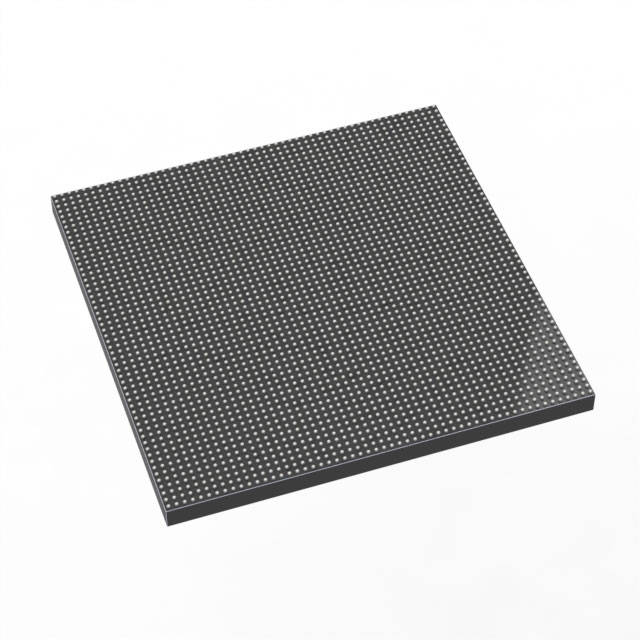
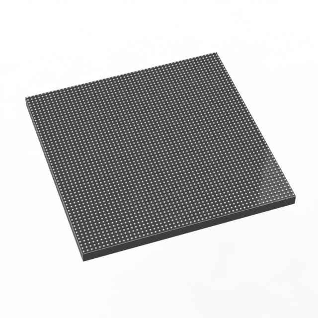
Stratix® 10 GX Field Programmable Gate Array (FPGA) IC 1160 2500000 2912-BBGA, FCBGA |
|---|---|
| Quantity | 390 Available (as of October 8, 2026) |
| Product Category | Field Programmable Gate Array (FPGA) |
|---|---|
| Manufacturer | Intel |
| Manufacturing Status | Active |
| Manufacturer Standard Lead Time | 12 Weeks |
| Datasheet |
Specifications & Environmental
| Device Package | 2912-FBGA, FC (55x55) | Grade | Extended | Operating Temperature | 0°C – 100°C | ||
|---|---|---|---|---|---|---|---|
| Package / Case | 2912-BBGA, FCBGA | Number of I/O | 1160 | Voltage | 820 mV - 880 mV | ||
| Mounting Method | Surface Mount | RoHS Compliance | Unknown | REACH Compliance | REACH Unaffected | ||
| Moisture Sensitivity Level | 3 (168 Hours) | Number of LABs/CLBs | 312500 | Number of Logic Elements/Cells | 2500000 | ||
| Number of Gates | N/A | ECCN | N/A | HTS Code | N/A | ||
| Qualification | N/A | Total RAM Bits | 204472320 |
Overview of 1SG250HH2F55E2LG – Stratix® 10 GX Field Programmable Gate Array (FPGA) IC
The 1SG250HH2F55E2LG is an Intel Stratix® 10 GX family FPGA optimized for high-performance, high-bandwidth designs. It is built on the Stratix 10 architecture and the device family innovations described in the Intel Stratix 10 GX overview, including the Intel Hyperflex core architecture and Intel 14 nm tri-gate (FinFET) technology.
This device targets advanced communications and compute applications that require large logic capacity, extensive on-chip memory, and high I/O density while operating within a specified extended temperature and supply range.
Key Features
- Core & architecture Part of the Intel Stratix 10 GX family featuring the Intel Hyperflex core architecture and Intel 14 nm tri-gate (FinFET) process as described in the device overview.
- Logic capacity 2,500,000 logic elements, providing substantial programmable fabric for complex logic and compute functions.
- On-chip memory Total on-chip RAM of 204,472,320 bits to support large buffering, caching, and scratchpad needs within the FPGA fabric.
- I/O density 1,160 I/O pins for high fanout and connectivity to external devices, memory, and high-speed interfaces.
- Power supply Core voltage range specified at 820 mV to 880 mV for the device core supply.
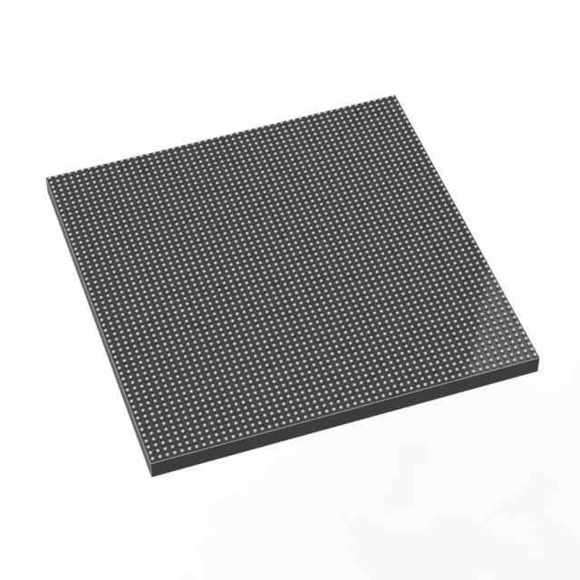
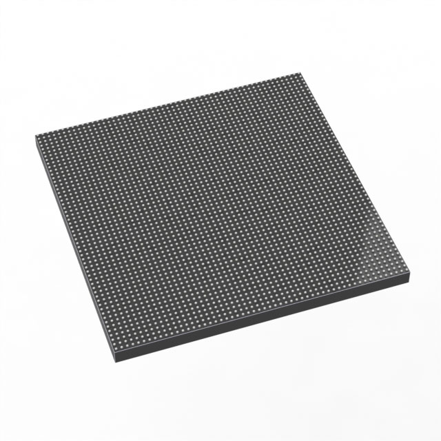
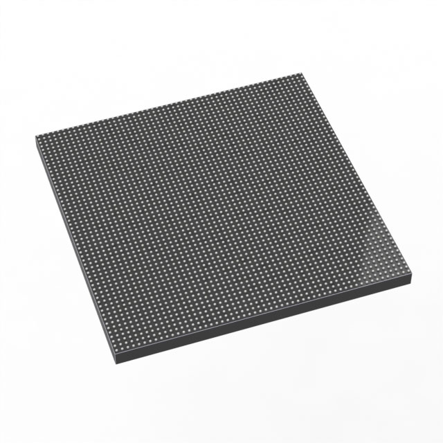
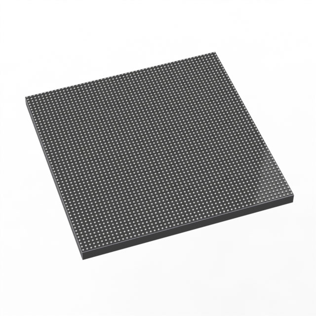
- Package & mounting Supplied in a 2912-BBGA (FCBGA) package; supplier device package listed as 2912-FBGA, FC (55×55). Surface-mount mounting type.
- Temperature & grade Extended-grade device with an operating temperature range of 0 °C to 100 °C.
- Compliance RoHS compliant.
- Stratix 10 GX family capabilities The Stratix 10 GX/SX family overview describes advanced family-level features available across devices, including high-performance transceiver and interface hard IP blocks, variable precision DSP resources, and embedded memory blocks (family-level functionality referenced from the device overview).
Typical Applications
- High-speed communications Use the device's high logic count and dense I/O for packet processing, backplane or module interfaces, and data-plane acceleration.
- Data center and networking Implement custom switching, bridging, or protocol offload functions where large on-chip RAM and extensive I/O are required.
- Signal processing and compute acceleration Leverage the large logic fabric and on-chip memory for real-time signal processing chains and algorithm acceleration.
Unique Advantages
- Large programmable fabric: 2,500,000 logic elements enable high-density logic implementation and complex system integration on a single device.
- Substantial on-chip RAM: 204,472,320 bits of RAM reduce dependency on external memory for buffering and improve deterministic data access.
- High I/O count: 1,160 I/O pins support extensive external connectivity and parallel interfaces without multiple devices.
- Advanced packaging: 2912-ball FCBGA package (55×55) provides the pin density required for large designs while supporting surface-mount assembly.
- Extended operating range: Extended-grade temperature rating (0 °C to 100 °C) aligns the device with a wide range of commercial and enterprise deployments.
- Verified compliance: RoHS compliance simplifies regulatory handling for lead-free production environments.
Why Choose 1SG250HH2F55E2LG?
The 1SG250HH2F55E2LG delivers a high-capacity Stratix 10 GX FPGA option for designs that require extensive logic, large on-chip memory, and high I/O density in a single surface-mount package. Its family-level architecture and core technologies position it for demanding communications, data center, and compute-acceleration tasks where integration and determinism matter.
For engineering teams and procurement evaluating a scalable, high-performance FPGA platform, this device offers a balance of programmable resources, package pin-count, and family-proven architecture to support long-term design goals and system-level consolidation.
Request a quote or submit an inquiry to receive pricing, availability, and technical support information for 1SG250HH2F55E2LG.





















Date Founded: 1968
Headquarters: Santa Clara, California, USA
Employees: 130,000+
Revenue: $54.23 Billion
Certifications and Memberships: ISO9001:2015, ISO14001:2015, ISO17025:2017, ISO27001:2022, ISO45001:2018, ISO50001:2018


