
1SG250HH2F55E1VG
| Part Description |
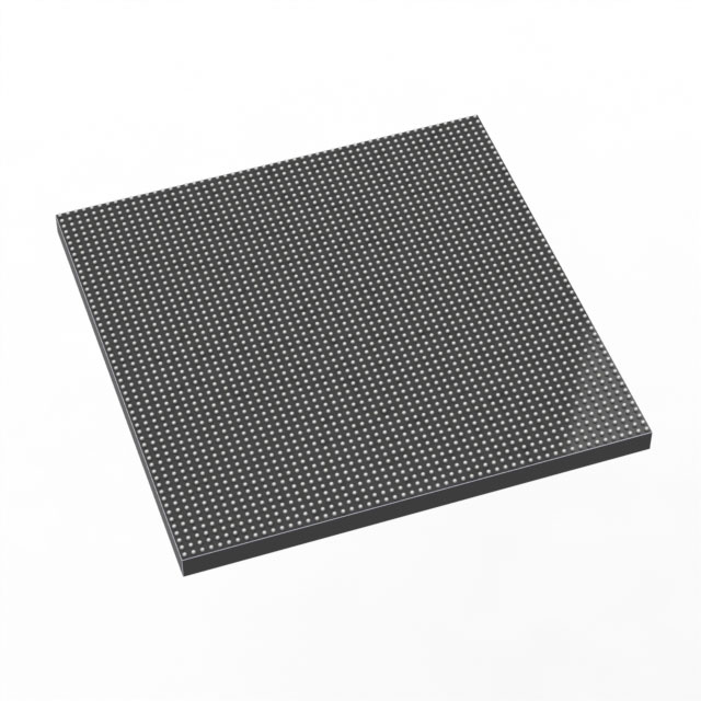
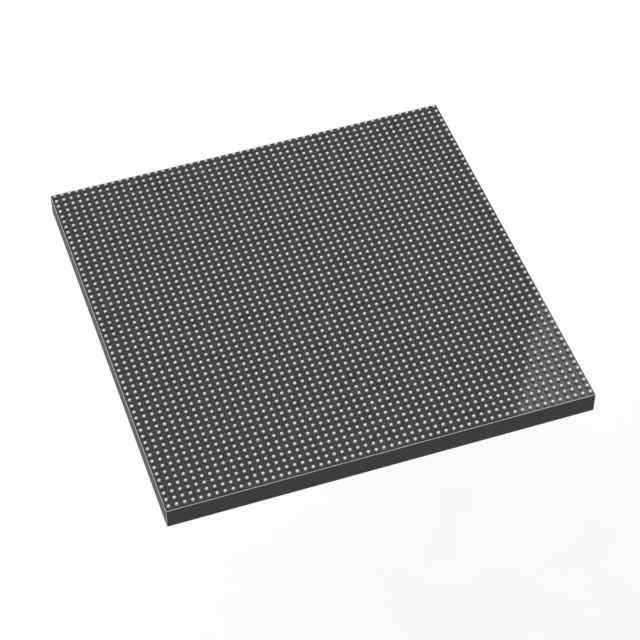
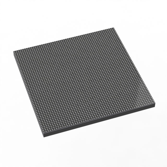
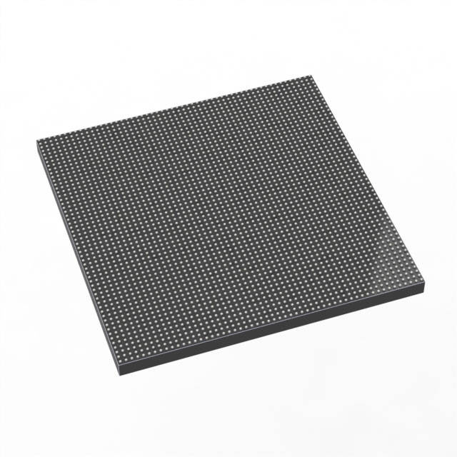
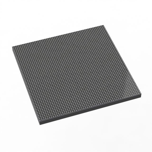
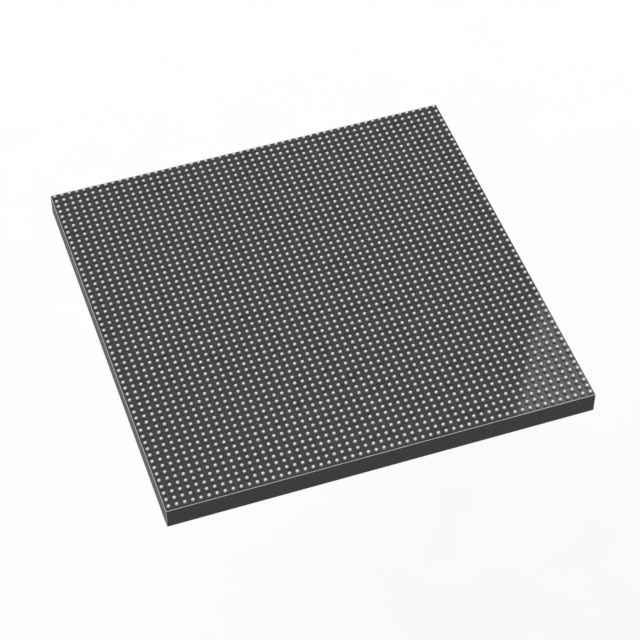
Stratix® 10 GX Field Programmable Gate Array (FPGA) IC 1160 2500000 2912-BBGA, FCBGA |
|---|---|
| Quantity | 235 Available (as of October 7, 2026) |
| Product Category | Field Programmable Gate Array (FPGA) |
|---|---|
| Manufacturer | Intel |
| Manufacturing Status | Active |
| Manufacturer Standard Lead Time | 12 Weeks |
| Datasheet |
Specifications & Environmental
| Device Package | 2912-FBGA, FC (55x55) | Grade | Extended | Operating Temperature | 0°C – 100°C | ||
|---|---|---|---|---|---|---|---|
| Package / Case | 2912-BBGA, FCBGA | Number of I/O | 1160 | Voltage | 770 mV - 970 mV | ||
| Mounting Method | Surface Mount | RoHS Compliance | Unknown | REACH Compliance | REACH Unaffected | ||
| Moisture Sensitivity Level | 3 (168 Hours) | Number of LABs/CLBs | 312500 | Number of Logic Elements/Cells | 2500000 | ||
| Number of Gates | N/A | ECCN | N/A | HTS Code | N/A | ||
| Qualification | N/A | Total RAM Bits | 204472320 |
Overview of 1SG250HH2F55E1VG – Stratix® 10 GX FPGA IC, 2,500,000 logic elements, 2912-BBGA
The 1SG250HH2F55E1VG is an Intel Stratix® 10 GX field programmable gate array (FPGA) offered in a 2912-BBGA FCBGA package. This device implements the Stratix 10 family architecture, featuring the Intel Hyperflex™ core and Intel 14 nm tri-gate (FinFET) technology to address high-bandwidth, compute-intensive applications.
With 2,500,000 logic elements, extensive on-chip RAM, a high I/O count and low-voltage core supply, the device is positioned for demanding applications that require large logic capacity, high I/O density, and robust system-level integration.
Key Features
- Core Architecture Built on the Intel Hyperflex™ core architecture and 14 nm tri-gate (FinFET) process, delivering improved core performance for compute- and bandwidth-intensive designs.
- Logic Density Contains 2,500,000 logic elements (cells), enabling complex logic implementations and large-scale FPGA designs.
- On‑Chip Memory Provides 204,472,320 total RAM bits of internal memory to support large buffering, lookup tables, and embedded data structures.
- I/O Capacity Offers 1,160 I/O pins to support broad peripheral, memory, and high-speed interface connectivity requirements.
- Transceiver and High‑Speed I/O Technologies As part of the Stratix 10 GX family, the architecture includes advanced transceiver and PCS/PMA features designed to support high-speed serial links and protocol IP common to the family.
- Power and Voltage Operates with a core voltage supply range of 770 mV to 970 mV, enabling power-scalable system designs.
- Package and Mounting Supplied in a 2912-FBGA (55 × 55 mm) package, surface mount (FCBGA) for compact board-level integration.
- Temperature and Grade Extended grade device with an operating temperature range of 0 °C to 100 °C for a wide variety of commercial and enterprise environments.
- Family Innovations Stratix 10 family innovations noted in the device overview include fractional synthesis PLLs, variable precision DSP blocks, hard memory controllers and protocol IP such as PCI Express and Ethernet in family variants.
Typical Applications
- High‑Speed Networking Used where high I/O density and advanced transceiver capabilities are required for switching, routing, or line-card applications.
- Data Center Acceleration Suited for hardware acceleration and offload tasks that leverage large logic capacity and substantial on-chip RAM for buffering and compute kernels.
- Telecommunications Infrastructure Ideal for protocol processing, line-rate packet processing, and other telecom functions that require deterministic I/O and high logic density.
- Advanced Signal Processing Applicable to DSP-heavy workloads that take advantage of the Stratix 10 family’s variable precision DSP capabilities and large internal memory.
Unique Advantages
- High Logic Capacity: 2,500,000 logic elements enable implementation of large, complex designs without external partitioning.
- Substantial On‑Chip Memory: 204,472,320 bits of RAM reduce dependence on external memory for many buffering and state-storage needs.
- Extensive I/O Count: 1,160 I/Os support multiple high-density interfaces and parallel connectivity on a single device.
- Low-Voltage Core Supply: 770 mV to 970 mV core voltage range allows designers to optimize performance versus power within the supported range.
- Board-Level Integration: 2912-FBGA (55 × 55 mm) surface-mount package supports compact, high-density board designs.
- Extended Grade Operation: 0 °C to 100 °C operating range suitable for a broad set of commercial and enterprise deployments.
Why Choose 1SG250HH2F55E1VG?
The 1SG250HH2F55E1VG combines the Stratix 10 GX family’s Hyperflex core architecture and 14 nm FinFET technology with device-level resources—2.5 million logic elements, over 204 million bits of on-chip RAM, and 1,160 I/Os—to address high-performance, high-bandwidth system designs. Its package and extended temperature grade support integration into compact, robust boards for communications, data center, and signal-processing applications.
This device is suited to design teams that need substantial programmable logic capacity and large internal memory within a single FPGA package, enabling consolidation of functions and reducing external component count while operating within a low-voltage core envelope.
Request a quote or submit an inquiry for pricing and availability for the 1SG250HH2F55E1VG to receive further information tailored to your project requirements.





















Date Founded: 1968
Headquarters: Santa Clara, California, USA
Employees: 130,000+
Revenue: $54.23 Billion
Certifications and Memberships: ISO9001:2015, ISO14001:2015, ISO17025:2017, ISO27001:2022, ISO45001:2018, ISO50001:2018


