
1SG250HH2F55I2LG
| Part Description |
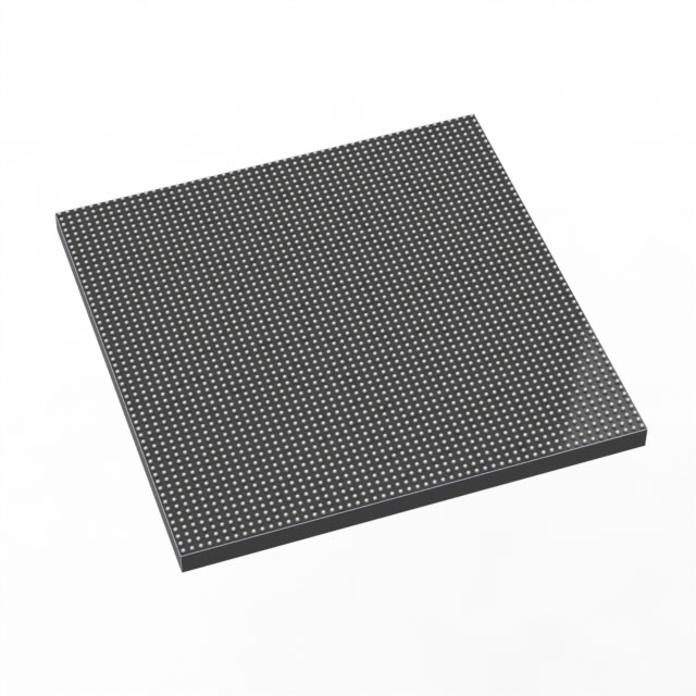
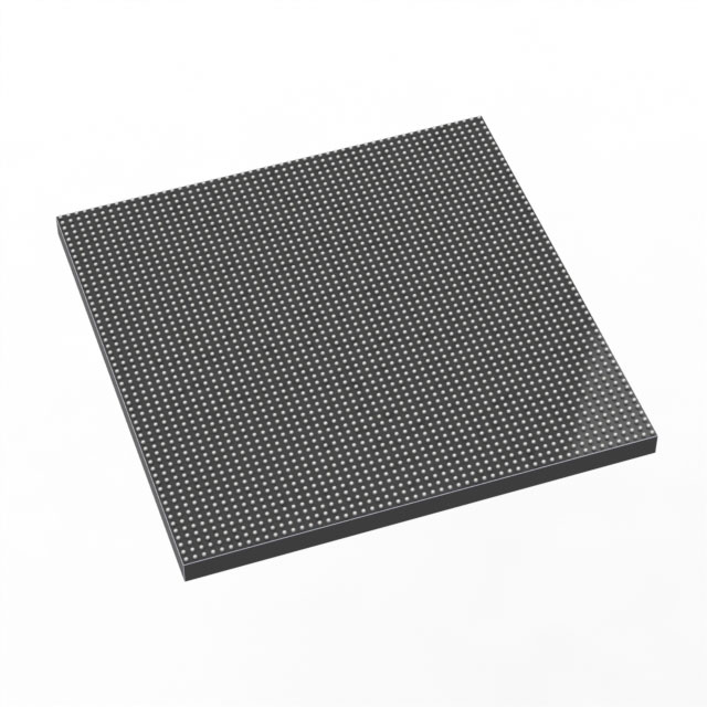
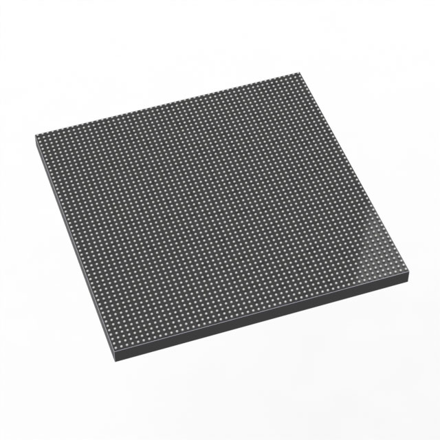
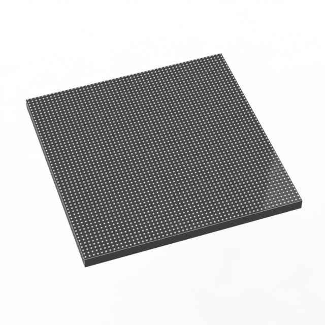
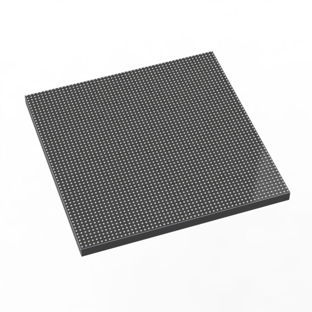
Stratix® 10 GX Field Programmable Gate Array (FPGA) IC 1160 2500000 2912-BBGA, FCBGA |
|---|---|
| Quantity | 1,236 Available (as of October 8, 2026) |
| Product Category | Field Programmable Gate Array (FPGA) |
|---|---|
| Manufacturer | Intel |
| Manufacturing Status | Active |
| Manufacturer Standard Lead Time | 12 Weeks |
| Datasheet |
Specifications & Environmental
| Device Package | 2912-FBGA, FC (55x55) | Grade | Industrial | Operating Temperature | -40°C – 100°C | ||
|---|---|---|---|---|---|---|---|
| Package / Case | 2912-BBGA, FCBGA | Number of I/O | 1160 | Voltage | 820 mV - 880 mV | ||
| Mounting Method | Surface Mount | RoHS Compliance | Unknown | REACH Compliance | REACH Unaffected | ||
| Moisture Sensitivity Level | 3 (168 Hours) | Number of LABs/CLBs | 312500 | Number of Logic Elements/Cells | 2500000 | ||
| Number of Gates | N/A | ECCN | N/A | HTS Code | N/A | ||
| Qualification | N/A | Total RAM Bits | 204472320 |
Overview of 1SG250HH2F55I2LG – Stratix® 10 GX Field Programmable Gate Array, 2912‑BBGA FCBGA
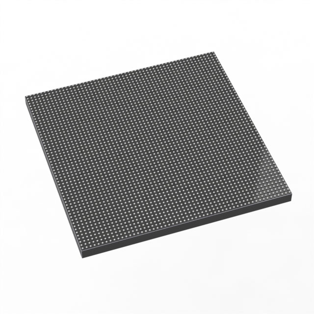
The 1SG250HH2F55I2LG is an Intel Stratix® 10 GX FPGA in a 2912‑ball FCBGA package, designed for high‑performance, high‑bandwidth applications. It combines a large configurable fabric with industry‑grade operating range and a compact surface‑mount package for deployment in demanding embedded and communications systems.
As a member of the Stratix 10 GX family, this device targets advanced applications requiring significant logic capacity, on‑chip memory, and extensive I/O while meeting industrial temperature and RoHS compliance requirements.
Key Features
- Core architecture (family): Stratix 10 GX family innovations include the Intel Hyperflex™ core architecture and Intel 14 nm tri‑gate (FinFET) technology, delivering improved core performance and power efficiency at the family level.
- Logic capacity: 2,500,000 logic elements (cells) providing large-scale programmable logic resources for complex designs.
- Embedded memory: 204,472,320 total RAM bits for on‑chip buffering, state storage, and large LUT‑based structures.
- I/O density: 1,160 I/O pins to support broad connectivity and multiple high‑speed interfaces.
- Package and mounting: 2912‑BBGA (FCBGA) package; supplier device package 2912‑FBGA, FC (55×55); surface mount for board‑level integration.
- Power supply: Core voltage supply specified at 820 mV to 880 mV for predictable power planning.
- Operating temperature: Industrial operating range of −40 °C to 100 °C for deployment in temperature‑challenging environments.
- Environmental compliance: RoHS compliant to meet regulatory requirements for lead‑free manufacturing.
Typical Applications
- High‑performance networking: Large logic capacity and extensive I/O make this device suitable for packet processing, switching, and custom protocol offload functions.
- Data center and accelerators: On‑chip memory and dense logic support complex data‑path implementations and custom compute kernels.
- Telecommunications equipment: Industrial temperature grade and high I/O count enable use in line cards, optical modules, and aggregation systems.
Unique Advantages
- Massive programmable fabric: 2.5 million logic elements let you implement large, consolidated designs on a single device, reducing board count and system complexity.
- Large on‑chip memory: Over 204 million bits of RAM permit extensive buffering and state retention without external memory for many use cases.
- High I/O count: 1,160 I/Os support multiple parallel interfaces and high fan‑out connectivity for complex system designs.
- Industrial reliability: −40 °C to 100 °C operating range and surface‑mount FCBGA package support deployment in harsh and industrial environments.
- Predictable power planning: Defined core voltage range (820–880 mV) simplifies power supply design and thermal budgeting.
- Regulatory readiness: RoHS compliance supports lead‑free manufacturing workflows and regulatory conformity.
Why Choose 1SG250HH2F55I2LG?
The 1SG250HH2F55I2LG positions itself for designs that require large programmable capacity, substantial on‑chip memory, and broad I/O in an industrial‑grade FPGA package. Its specification set supports integration into high‑bandwidth networking, telecommunications, and data center hardware where consolidation of functionality and reliable operation across a wide temperature range are essential.
Choosing this Stratix 10 GX device gives development teams access to the family’s core architectural innovations and high resource counts, enabling scalable designs with long‑term maintainability, predictable power requirements, and RoHS‑compliant manufacturing.
Request a quote or submit an inquiry to receive pricing and availability information for the 1SG250HH2F55I2LG.





















Date Founded: 1968
Headquarters: Santa Clara, California, USA
Employees: 130,000+
Revenue: $54.23 Billion
Certifications and Memberships: ISO9001:2015, ISO14001:2015, ISO17025:2017, ISO27001:2022, ISO45001:2018, ISO50001:2018


