
1SG250HH3F55E2LG
| Part Description |
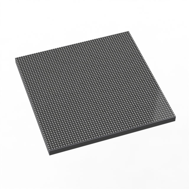
Stratix® 10 GX Field Programmable Gate Array (FPGA) IC 1160 2500000 2912-BBGA, FCBGA |
|---|---|
| Quantity | 34 Available (as of October 8, 2026) |
| Product Category | Field Programmable Gate Array (FPGA) |
|---|---|
| Manufacturer | Intel |
| Manufacturing Status | Active |
| Manufacturer Standard Lead Time | 12 Weeks |
| Datasheet |
Specifications & Environmental
| Device Package | 2912-FBGA, FC (55x55) | Grade | Extended | Operating Temperature | 0°C – 100°C | ||
|---|---|---|---|---|---|---|---|
| Package / Case | 2912-BBGA, FCBGA | Number of I/O | 1160 | Voltage | 820 mV - 880 mV | ||
| Mounting Method | Surface Mount | RoHS Compliance | Unknown | REACH Compliance | REACH Unaffected | ||
| Moisture Sensitivity Level | 3 (168 Hours) | Number of LABs/CLBs | 312500 | Number of Logic Elements/Cells | 2500000 | ||
| Number of Gates | N/A | ECCN | N/A | HTS Code | N/A | ||
| Qualification | N/A | Total RAM Bits | 204472320 |
Overview of 1SG250HH3F55E2LG – Stratix® 10 GX FPGA, 2,500,000 logic elements, 2912-BBGA
The 1SG250HH3F55E2LG is an Intel Stratix® 10 GX Field Programmable Gate Array supplied in a high‑pin‑count 2912‑BBGA package. This device combines a high‑density programmable fabric with the Stratix 10 family innovations to address advanced, high‑bandwidth system designs.
With 2,500,000 logic elements, 204,472,320 bits of on‑chip RAM and 1,160 I/O pins, the device is targeted at applications demanding large logic capacity, extensive I/O, and significant embedded memory. The part is supplied in a surface‑mount, extended‑grade package and is RoHS compliant.
Key Features
- Logic Fabric The device provides 2,500,000 logic elements to implement complex, high‑capacity designs.
- On‑chip Memory 204,472,320 total RAM bits for large buffer, packet and data‑processing requirements; the Stratix 10 family documentation references M20K internal SRAM blocks for embedded memory building blocks.
- I/O and High‑Speed Connectivity 1,160 I/O pins for dense external interfacing. Stratix 10 GX family materials document heterogeneous transceiver tiles and high‑speed serial capabilities for demanding link requirements.
- Core Architecture Built on the Stratix 10 GX family architecture, which the documentation highlights for Intel Hyperflex core architecture and Intel 14 nm tri‑gate technology to support high performance and power efficiency at the device family level.
- Power Supply Core voltage supply range of 820 mV to 880 mV, enabling optimized core power operation within specified limits.
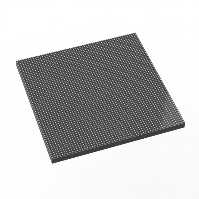
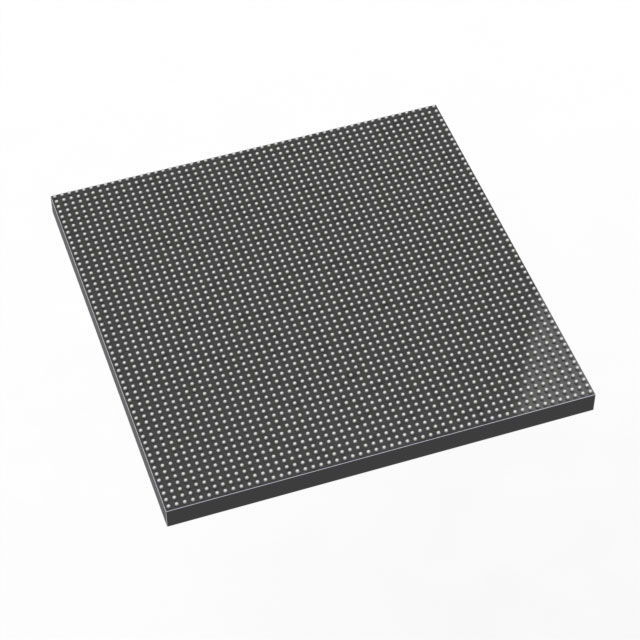
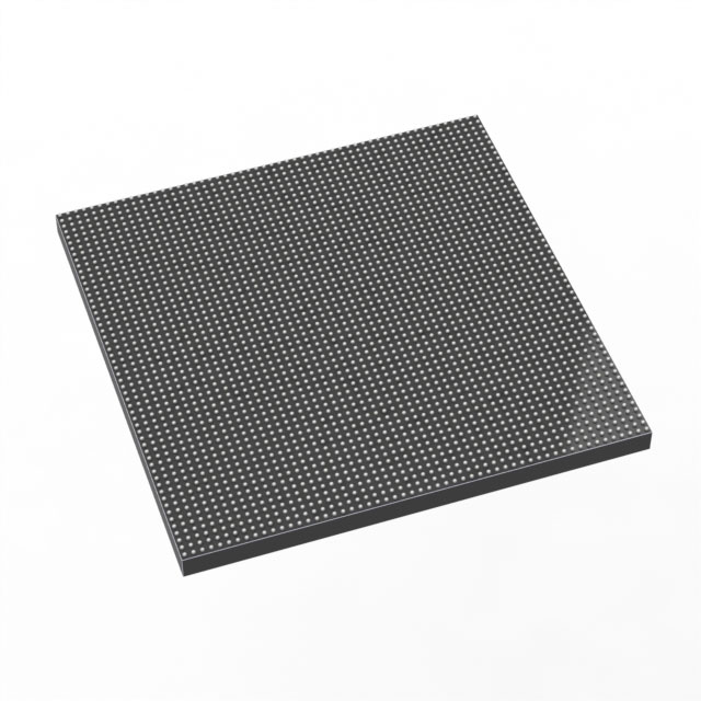
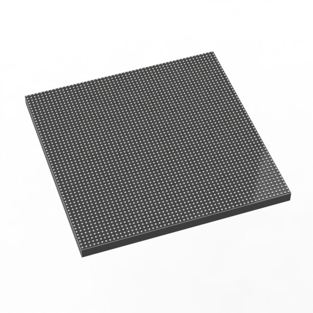
- Package & Mounting 2912‑BBGA (FCBGA) package, supplier device package 2912‑FBGA, FC (55×55), designed for surface‑mount PCB assembly and high pin count system integration.
- Temperature & Grade Extended grade device with an operating temperature range of 0 °C to 100 °C.
- Standards & Reliability RoHS compliant. Stratix 10 family documentation includes device security, configuration features and single‑event upset (SEU) detection and correction capabilities.
Typical Applications
- High‑speed Networking & Switching Large logic density and extensive I/O support complex packet processing, protocol offload and line‑rate switching functions.
- Data Center Acceleration Large on‑chip RAM and high logic capacity enable custom acceleration engines for storage, compression, and pattern matching workloads.
- Telecom & Optical Transport Family‑level transceiver and hard IP features support implementations for backplane, optical transport and aggregation equipment.
- Signal Processing & Compute Appliances The combination of dense logic and embedded memory supports wideband DSP pipelines and custom floating/fixed‑point processing engines.
Unique Advantages
- High Logic Density: 2,500,000 logic elements provide the capacity to consolidate complex SoC‑like functions into a single FPGA.
- Large Embedded Memory: 204,472,320 bits of on‑chip RAM reduce dependency on external memory for buffering and data staging.
- Extensive External Connectivity: 1,160 I/O pins accommodate high pin‑count interfaces and dense board‑level integration.
- Optimized Core Power: A tight core voltage range (820–880 mV) supports power‑aware system design and predictable core power delivery.
- High‑Pin‑Count, Surface‑Mount Package: 2912‑BBGA FCBGA package enables high signal density and compact system layouts.
- Extended Temperature Rating: 0 °C to 100 °C operating range for designs targeting extended commercial operating environments.
Why Choose 1SG250HH3F55E2LG?
The 1SG250HH3F55E2LG positions itself where large programmable capacity, significant embedded memory and broad I/O are required. It is suited for designers building high‑bandwidth networking, data center acceleration, telecom and advanced signal‑processing systems that need a high‑density FPGA in a high‑pin‑count surface‑mount package.
As a member of the Intel Stratix 10 GX family, the device aligns with documented family features such as Hyperflex core architecture and advanced transceiver and IP options, providing a pathway for scalable designs and integration within the Stratix 10 ecosystem.
Request a quote or submit an inquiry for pricing and availability of 1SG250HH3F55E2LG. Our team will provide the information needed to evaluate this device for your next design.






















Date Founded: 1968
Headquarters: Santa Clara, California, USA
Employees: 130,000+
Revenue: $54.23 Billion
Certifications and Memberships: ISO9001:2015, ISO14001:2015, ISO17025:2017, ISO27001:2022, ISO45001:2018, ISO50001:2018


