
1SG250HH3F55E3XG
| Part Description |
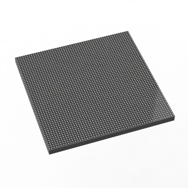
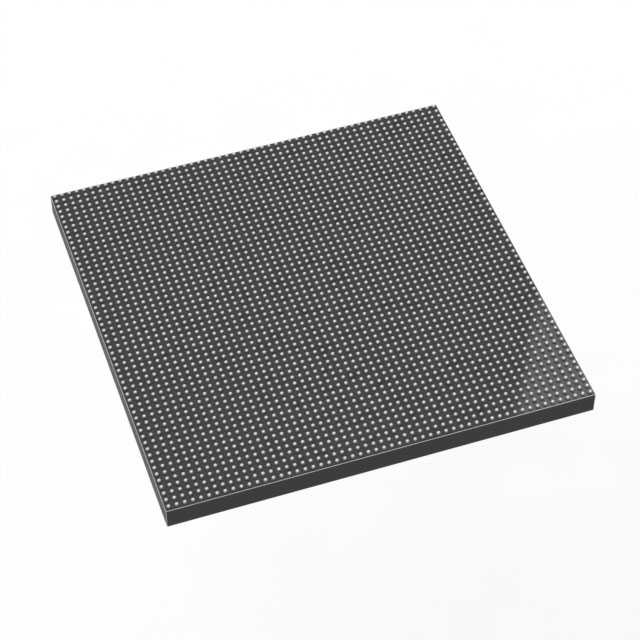
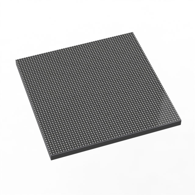
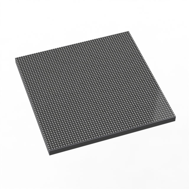
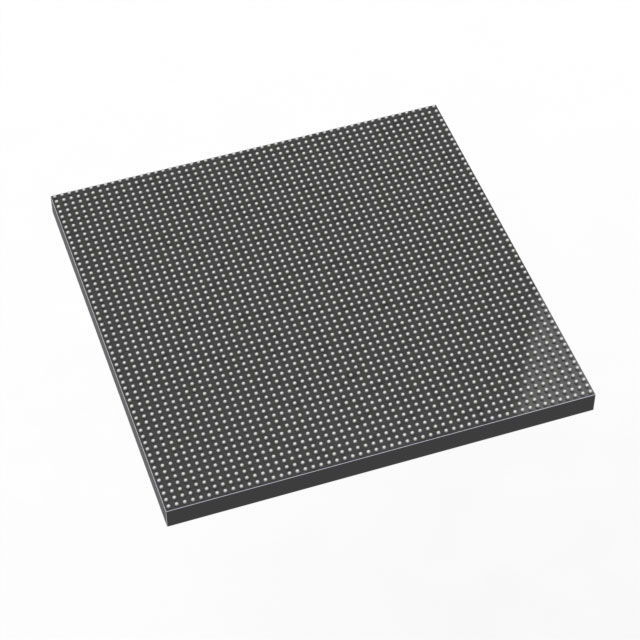
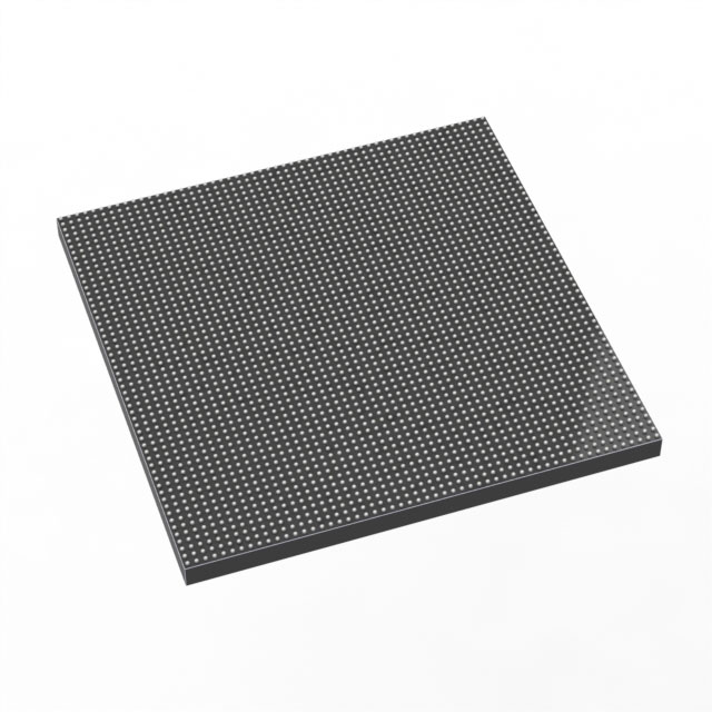
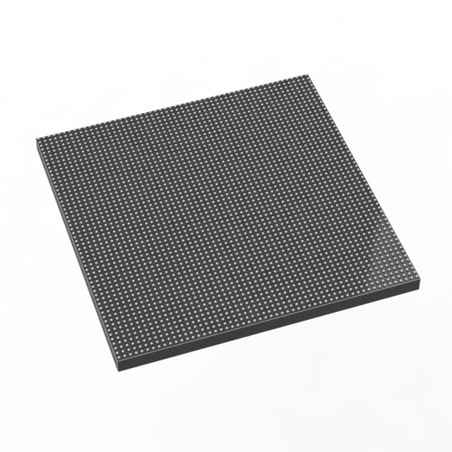
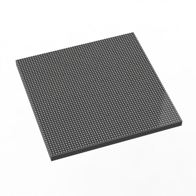
Stratix® 10 GX Field Programmable Gate Array (FPGA) IC 1160 2500000 2912-BBGA, FCBGA |
|---|---|
| Quantity | 1,594 Available (as of October 8, 2026) |

| Product Category | Field Programmable Gate Array (FPGA) |
|---|---|
| Manufacturer | Intel |
| Manufacturing Status | Active |
| Manufacturer Standard Lead Time | 12 Weeks |
| Datasheet |
Specifications & Environmental
| Device Package | 2912-FBGA, FC (55x55) | Grade | Extended | Operating Temperature | 0°C – 100°C | ||
|---|---|---|---|---|---|---|---|
| Package / Case | 2912-BBGA, FCBGA | Number of I/O | 1160 | Voltage | 820 mV - 880 mV | ||
| Mounting Method | Surface Mount | RoHS Compliance | Unknown | REACH Compliance | REACH Unaffected | ||
| Moisture Sensitivity Level | 3 (168 Hours) | Number of LABs/CLBs | 312500 | Number of Logic Elements/Cells | 2500000 | ||
| Number of Gates | N/A | ECCN | N/A | HTS Code | N/A | ||
| Qualification | N/A | Total RAM Bits | 204472320 |
Overview of 1SG250HH3F55E3XG – Stratix® 10 GX Field Programmable Gate Array (FPGA) IC
The 1SG250HH3F55E3XG is a Stratix® 10 GX family FPGA offering very large programmable logic capacity and advanced on‑chip resources for demanding bandwidth and compute applications. It leverages the Stratix 10 family innovations, including the Intel Hyperflex core architecture and 14 nm tri‑gate (FinFET) technology, to address high‑performance networking, compute acceleration, and SoC integration use cases.
Designed for surface‑mount implementation in a 2912‑BBGA (2912‑FBGA, 55×55) package, this device combines 2,500,000 logic elements, extensive embedded memory, and a broad I/O count to support complex, high‑density designs within an extended temperature grade.
Key Features
- Core Architecture Intel Hyperflex core architecture and 14 nm tri‑gate (FinFET) process deliver the family performance and power efficiency characteristics described for Stratix 10 GX devices.
- Logic Capacity 2,500,000 logic elements to implement large, highly parallel designs and complex system functions.
- Embedded Memory 204,472,320 total RAM bits of on‑chip memory for buffering, caching, and data‑path storage.
- I/O and High‑Speed Interfaces 1,160 user I/O pins for flexible system interfacing. The Stratix 10 family also provides heterogeneous 3D SiP transceiver tiles and family transceiver capabilities suitable for high‑bandwidth links.
- Hard IP and DSP Family‑level hard IP options include PCI Express Gen3 x16 and hardened Ethernet/forward error correction; variable‑precision DSP blocks provide dense compute resources for signal processing workloads.
- Package, Power and Mounting Surface mount device in a 2912‑BBGA (2912‑FBGA, 55×55) package. Core supply range specified at 820 mV to 880 mV.
- Operating Range and Grade Extended grade operation with an ambient range of 0 °C to 100 °C.
- Environmental Compliance RoHS compliant.
Typical Applications
- High‑Performance Networking and Switches — Deploy large logic capacity, extensive on‑chip memory, and high‑speed I/O for packet processing, traffic management, and line‑rate feature acceleration.
- Data Center Acceleration — Use dense DSP and logic resources to implement compute‑intensive accelerators and offload functions from CPUs in data‑center environments.
- Telecommunications and Optical Transport — Leverage family transceiver capabilities and hardened protocol IP for backplane and optical line cards requiring high bandwidth and low latency.
- SoC and Embedded Processing — Integrate programmable fabric with SoC features available across the Stratix 10 family for complex embedded control, packet processing, and system partitioning.
Unique Advantages
- Highly Scalable Logic Fabric: 2.5M logic elements enable large centralized designs or many parallel hardware accelerators on a single device.
- Large On‑Chip Memory: Over 204Mbits of embedded RAM reduces external memory dependence and improves data locality for high‑throughput designs.
- Extensive I/O Count: 1,160 I/O pins provide flexible connectivity for dense board designs and multiple interface standards.
- Advanced Process and Architecture: Stratix 10 family innovations (Hyperflex and 14 nm FinFET) provide a balance of performance and power for sustained high‑compute tasks.
- Robust Packaging for Surface Mount Assembly: 2912‑FBGA (55×55) package supports high‑density PCB integration while meeting extended temperature requirements.
- Compliance and Production Readiness: RoHS compliance supports environmental regulatory requirements for deployment.
Why Choose 1SG250HH3F55E3XG?
1SG250HH3F55E3XG positions designers to implement very large, bandwidth‑intensive systems by combining massive logic capacity, substantial embedded memory, and broad I/O in a single Stratix 10 GX FPGA package. Its extended temperature grade and surface‑mount BGA packaging make it suitable for high‑density board designs that require sustained performance.
This device is best suited for engineering teams developing high‑performance networking, telecom, data‑center acceleration, or SoC‑style embedded systems who need the capacity and architectural advantages provided by the Stratix 10 family.
To request a quote or submit an inquiry for 1SG250HH3F55E3XG, please provide the part number and your project requirements to receive pricing and availability information.





















Date Founded: 1968
Headquarters: Santa Clara, California, USA
Employees: 130,000+
Revenue: $54.23 Billion
Certifications and Memberships: ISO9001:2015, ISO14001:2015, ISO17025:2017, ISO27001:2022, ISO45001:2018, ISO50001:2018


