
1SG250HH3F55I2VG
| Part Description |
Stratix® 10 GX Field Programmable Gate Array (FPGA) IC 1160 2500000 2912-BBGA, FCBGA |
|---|---|
| Quantity | 87 Available (as of June 14, 2026) |

| Product Category | Field Programmable Gate Array (FPGA) |
|---|---|
| Manufacturer | Intel |
| Manufacturing Status | Active |
| Manufacturer Standard Lead Time | 12 Weeks |
| Datasheet |
Specifications & Environmental
| Device Package | 2912-FBGA, FC (55x55) | Grade | Industrial | Operating Temperature | -40°C – 100°C | ||
|---|---|---|---|---|---|---|---|
| Package / Case | 2912-BBGA, FCBGA | Number of I/O | 1160 | Voltage | 770 mV - 970 mV | ||
| Mounting Method | Surface Mount | RoHS Compliance | Unknown | REACH Compliance | REACH Unaffected | ||
| Moisture Sensitivity Level | 3 (168 Hours) | Number of LABs/CLBs | 312500 | Number of Logic Elements/Cells | 2500000 | ||
| Number of Gates | N/A | ECCN | N/A | HTS Code | N/A | ||
| Qualification | N/A | Total RAM Bits | 204472320 |
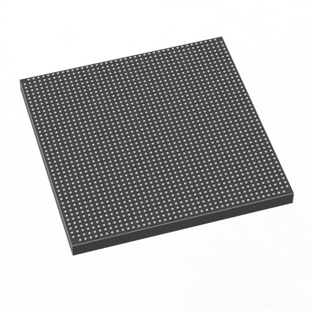
Overview of 1SG250HH3F55I2VG – Stratix® 10 GX FPGA, 2,500,000 logic elements, 1160 I/Os, 2912-BBGA
The 1SG250HH3F55I2VG is an Intel Stratix® 10 GX field programmable gate array (FPGA) IC designed for high-performance, industrial-grade applications. Built on the Stratix 10 family architecture, the device combines the Intel Hyperflex™ core architecture and Intel 14 nm tri-gate (FinFET) process innovations to address demanding bandwidth and processing requirements.
With 2,500,000 logic elements, 204,472,320 total RAM bits and 1,160 user I/Os in a 2912-BBGA FCBGA package, this FPGA is targeted at systems that require large programmable fabric, substantial on-chip memory and high I/O density while operating across an industrial temperature range.
Key Features
- Core Architecture Intel Hyperflex™ core architecture on 14 nm tri-gate (FinFET) technology, delivering the family-level performance improvements documented for Stratix 10 GX devices.
- Logic Capacity 2,500,000 logic elements for complex custom logic, large-scale state machines and wide datapath implementations.
- On‑Chip Memory 204,472,320 total RAM bits with family support for internal M20K SRAM memory blocks to implement large buffers, FIFOs and on-chip storage.
- High‑Density I/O 1,160 I/O pins to support broad external connectivity and high channel counts in dense system designs.
- Transceivers & Interface IP (Family) Stratix 10 GX family includes high-speed transceiver and hard IP options such as PCIe Gen3 and 10G Ethernet FEC, enabling high-bandwidth chip-to-chip and backplane interfaces (family-level capabilities).
- Package & Mounting Surface-mount 2912-BBGA (supplier device package: 2912-FBGA, FC 55×55) for high pin-count board designs.
- Power Core supply range 770 mV to 970 mV, enabling integration into tightly managed power budgets.
- Environmental & Thermal Industrial grade device with an operating temperature range of −40 °C to 100 °C and RoHS compliance for environmental conformity.
- Security & Reliability (Family) Family-level features include secure device management, error detection/correction and support for partial/dynamic reconfiguration to help maintain system reliability.
Typical Applications
- High‑Performance Networking Use the large logic capacity and high I/O density for packet processing, switch/router line cards and backplane interface logic.
- Data Center Acceleration Implement custom acceleration, protocol offload and high-bandwidth interconnect logic leveraging extensive on-chip memory and family transceiver options.
- Telecom & Optical Transport Support for high-speed transceivers and forward error correction at the family level makes this device suitable for transport and aggregation equipment.
- Industrial Systems Industrial-grade temperature range and robust I/O count enable deployment in demanding control, instrumentation and processing systems.
Unique Advantages
- Massive Logic Density: 2,500,000 logic elements provide headroom for large, complex FPGA designs without partitioning into multiple devices.
- Large On‑Chip Memory: Over 204 million RAM bits let you implement deep buffers, large lookup tables and memory-centric algorithms on-chip to reduce external memory dependence.
- High I/O Count: 1,160 I/Os simplify board-level routing for multi-channel systems and dense interface requirements.
- Industrial Temperature Range: Rated from −40 °C to 100 °C for deployment in industrial environments where extended thermal tolerance is required.
- Advanced Family-Level IP: Stratix 10 GX family features such as Hyperflex architecture, high-speed transceiver support and hard PCIe/ethernet IP provide a platform for high-performance system designs.
- Designed for Complex Systems: Surface-mount 2912-BBGA packaging supports high pin-count, space-efficient board designs.
Why Choose 1SG250HH3F55I2VG?
The 1SG250HH3F55I2VG delivers a combination of very high logic capacity, substantial on-chip memory and a large I/O complement in an industrial-grade Stratix 10 GX device. It is suited for engineers developing high-bandwidth networking equipment, data center accelerators, telecom infrastructure and industrial processing systems that require a robust, high-performance programmable fabric.
Backed by Stratix 10 family architectural advances and device-level specifications such as core voltage range, package details and operating temperature, this FPGA offers a scalable platform for advanced designs that need significant on-chip resources and proven family-level interface IP.
Request a quote or submit an inquiry to receive pricing, availability and technical support information for 1SG250HH3F55I2VG.


Date Founded: 1968
Headquarters: Santa Clara, California, USA
Employees: 130,000+
Revenue: $54.23 Billion
Certifications and Memberships: ISO9001:2015, ISO14001:2015, ISO17025:2017, ISO27001:2022, ISO45001:2018, ISO50001:2018


