
1SG250HN3F43I2LG
| Part Description |
Stratix® 10 GX Field Programmable Gate Array (FPGA) IC 688 2500000 1760-BBGA, FCBGA |
|---|---|
| Quantity | 1,360 Available (as of June 15, 2026) |

| Product Category | Field Programmable Gate Array (FPGA) |
|---|---|
| Manufacturer | Intel |
| Manufacturing Status | Active |
| Manufacturer Standard Lead Time | 12 Weeks |
| Datasheet |
Specifications & Environmental
| Device Package | 1760-FBGA (42.5x42.5) | Grade | Industrial | Operating Temperature | -40°C – 100°C | ||
|---|---|---|---|---|---|---|---|
| Package / Case | 1760-BBGA, FCBGA | Number of I/O | 688 | Voltage | 820 mV - 880 mV | ||
| Mounting Method | Surface Mount | RoHS Compliance | Unknown | REACH Compliance | REACH Unaffected | ||
| Moisture Sensitivity Level | 3 (168 Hours) | Number of LABs/CLBs | 312500 | Number of Logic Elements/Cells | 2500000 | ||
| Number of Gates | N/A | ECCN | N/A | HTS Code | N/A | ||
| Qualification | N/A | Total RAM Bits | 204472320 |
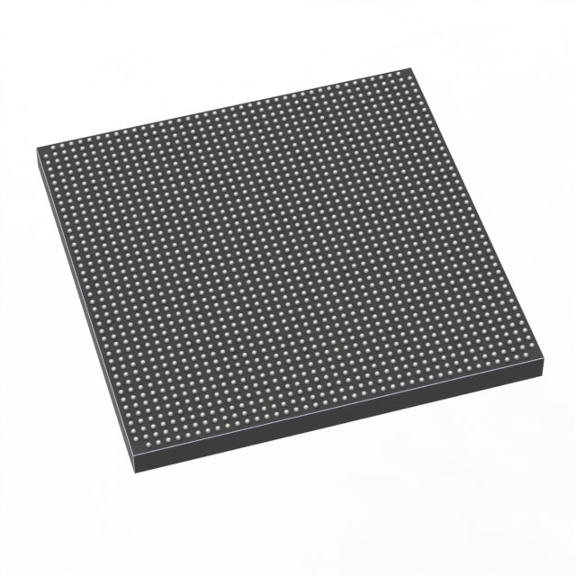
Overview of 1SG250HN3F43I2LG – Stratix® 10 GX FPGA, 2,500,000 logic elements, 688 I/O
The 1SG250HN3F43I2LG is an Intel Stratix® 10 GX field programmable gate array (FPGA) in a 1760‑BBGA (FCBGA) package designed for high-capacity, high-bandwidth applications. Built on the Stratix 10 family architecture, this device delivers large logic and memory resources alongside extensive I/O to address demanding communications, data center acceleration, and high-performance signal processing designs.
As an industrial‑grade device, it combines substantial on-chip RAM, a wide I/O count, and fine-grain power control to support designs that require dense programmable logic, robust I/O connectivity, and operation across a broad temperature range.
Key Features
- Core architecture: Stratix 10 family innovations including the Intel Hyperflex core architecture and Intel 14 nm tri‑gate (FinFET) process are referenced for this device family, providing the architectural foundation for high core performance.
- Logic capacity: 2,500,000 logic elements (logic resource count) to implement large, complex designs.
- On‑chip memory: 204,472,320 total RAM bits of embedded memory; the family also uses M20K internal SRAM memory blocks as part of its memory architecture.
- I/O and transceiver capability: 688 I/O pins available; Stratix 10 family transceivers support high data‑rate operation (family-referenced transceiver capabilities up to 28.3 Gbps for chip‑to‑chip/module and backplane links).
- Power supply range: Core voltage supply range 820 mV to 880 mV, enabling designers to plan power distribution and sequencing precisely.
- Package and mounting: Surface mount 1760‑BBGA (FCBGA) package; supplier device package listed as 1760‑FBGA with 42.5 × 42.5 mm footprint.
- Industrial temperature rating: Operating temperature range −40 °C to 100 °C, suitable for industrial environments.
- Device reliability and security (family features): Stratix 10 family documentation references device security, Single Event Upset (SEU) error detection and correction, and other reliability features available within the family architecture.
- Standards and compliance: RoHS compliant.
Typical Applications
- High‑speed networking and telecom: Use the device’s large logic capacity and family transceiver capabilities to implement packet processing, line cards, and protocol acceleration in high‑bandwidth systems.
- Data center acceleration: Leverage dense logic and large on‑chip memory for hardware acceleration tasks such as custom compute kernels, encryption, and I/O offload.
- Signal processing and test equipment: Implement complex DSP pipelines and real‑time processing chains using the device’s logic and memory resources.
- Embedded computing (family SoC variants): For Stratix 10 SoC family variants, integrated embedded processing options allow consolidation of control and data‑path functions; the family documentation references Arm‑based SoC variants when embedded processors are required.
Unique Advantages
- Extremely large programmable capacity: 2.5 million logic elements allow integration of complex systems and reduction of external components.
- Substantial on‑chip memory: Over 204 million bits of RAM enable large buffers, lookup tables, and state storage directly on the device.
- High I/O density: 688 I/O pins support wide parallel interfaces and dense board routing for complex system integration.
- Industrial robustness: Rated for −40 °C to 100 °C operation, suitable for industrial environments that require extended temperature range.
- Compact, industry‑grade packaging: 1760‑BBGA (42.5 × 42.5 mm) surface‑mount package balances large die capacity with standard assembly processes.
- Backed by Stratix 10 family architecture: Family‑level innovations such as Hyperflex core architecture, advanced FinFET process, and high‑speed transceiver technologies provide a well‑documented platform for high‑performance designs.
Why Choose 1SG250HN3F43I2LG?
The 1SG250HN3F43I2LG offers a combination of very high logic density, substantial embedded memory, and broad I/O capability in an industrial‑rated Stratix 10 GX device package. It is targeted at engineers building bandwidth‑intensive, compute‑heavy systems where consolidating functionality onto a single programmable device reduces BOM complexity and accelerates time to market.
Choosing this device means leveraging the Stratix 10 family architecture and documentation to scale designs from prototype to production while addressing industrial operating conditions and providing the resources needed for advanced networking, acceleration, and signal processing applications.
Request a quote or submit an inquiry to receive pricing, availability, and technical support information for part number 1SG250HN3F43I2LG.


Date Founded: 1968
Headquarters: Santa Clara, California, USA
Employees: 130,000+
Revenue: $54.23 Billion
Certifications and Memberships: ISO9001:2015, ISO14001:2015, ISO17025:2017, ISO27001:2022, ISO45001:2018, ISO50001:2018


