
1SG250HN3F43I3VG
| Part Description |
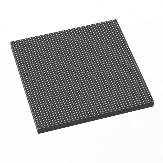
Stratix® 10 GX Field Programmable Gate Array (FPGA) IC 688 2500000 1760-BBGA, FCBGA |
|---|---|
| Quantity | 1,094 Available (as of June 15, 2026) |
| Product Category | Field Programmable Gate Array (FPGA) |
|---|---|
| Manufacturer | Intel |
| Manufacturing Status | Active |
| Manufacturer Standard Lead Time | 12 Weeks |
| Datasheet |
Specifications & Environmental
| Device Package | 1760-FBGA (42.5x42.5) | Grade | Industrial | Operating Temperature | -40°C – 100°C | ||
|---|---|---|---|---|---|---|---|
| Package / Case | 1760-BBGA, FCBGA | Number of I/O | 688 | Voltage | 770 mV - 970 mV | ||
| Mounting Method | Surface Mount | RoHS Compliance | Unknown | REACH Compliance | REACH Unaffected | ||
| Moisture Sensitivity Level | 3 (168 Hours) | Number of LABs/CLBs | 312500 | Number of Logic Elements/Cells | 2500000 | ||
| Number of Gates | N/A | ECCN | N/A | HTS Code | N/A | ||
| Qualification | N/A | Total RAM Bits | 204472320 |
Overview of 1SG250HN3F43I3VG – Stratix® 10 GX FPGA, 1760-BBGA
The 1SG250HN3F43I3VG is an Intel Stratix® 10 GX field programmable gate array (FPGA) supplied in a 1760‑FBGA (42.5 × 42.5 mm) surface‑mount package. It is built on the Stratix 10 family architecture and incorporates the Hyperflex core innovations and Intel 14 nm tri‑gate (FinFET) technology described for the family.
Designed for high‑performance, bandwidth‑intensive systems, this device offers 2,500,000 logic elements, extensive on‑chip RAM and 688 I/O pins, making it suited for advanced networking, compute acceleration, signal processing and SoC‑class designs where large FPGA fabric and industrial temperature operation are required.
Key Features
- Core & architecture Implements the Stratix 10 Hyperflex core architecture and Intel 14 nm tri‑gate (FinFET) process as described for the device family, delivering the architectural improvements detailed in the family overview.
- Logic capacity 2,500,000 logic elements provide large programmable fabric for complex custom logic, control and data‑path implementations.
- On‑chip memory 204,472,320 total RAM bits of internal memory support large buffering, lookup tables and state storage; the family also includes M20K internal SRAM memory blocks.
- I/O and package 688 I/O pins in a 1760‑FBGA (42.5 × 42.5 mm) FCBGA surface‑mount package enable wide peripheral connectivity and dense board routing.
- Power and supply Core voltage supply range from 770 mV to 970 mV, enabling operation within the specified low‑voltage core window.
- Industrial temperature range Rated for operation from −40 °C to 100 °C, supporting industrial applications and environments.
- High‑speed transceivers and connectivity (family capability) The Stratix 10 family includes high‑speed transceiver technology and hard IP for modern serial protocols; family documentation highlights multi‑Gbps transceiver performance and hard PCI Express and Ethernet IP options.
- DSP and compute resources (family capability) Family documentation cites variable precision DSP blocks and hard IP options to support intensive signal processing and compute tasks.
Typical Applications
- High‑performance networking Use in switches, routers and packet processors that require large programmable fabric, high I/O density and support for high‑speed serial connectivity.
- Data center and acceleration Suitable for compute acceleration and hardware offload tasks where substantial logic resources and on‑chip RAM enable custom data‑path and buffering implementations.
- Advanced signal processing Ideal for radar, communications and DSP applications that need wide parallelism, extensive internal memory and DSP block support from the family architecture.
- SoC and embedded platform prototyping Appropriate for designs leveraging Stratix 10 family features, including platforms integrating hard IP and SoC variants where applicable for system integration and prototyping.
Unique Advantages
- Extensive programmable capacity: 2,500,000 logic elements enable large, complex designs without partitioning across multiple devices.
- Large on‑chip RAM: 204,472,320 total RAM bits reduce dependence on external memory for buffering and fast local storage.
- High I/O density: 688 I/O pins in a single 1760‑FBGA package allow broad peripheral interfacing and high signal‑count implementations.
- Industrial temperature rating: −40 °C to 100 °C operation supports deployment in industrial and rugged environments.
- Low‑voltage core operation: 770 mV to 970 mV supply range aligns with advanced low‑voltage FPGA core domains for power‑aware designs.
- Stratix 10 family innovations: Family features such as the Hyperflex core architecture and FinFET process provide a platform foundation for higher performance and efficiency in demanding designs.
Why Choose 1SG250HN3F43I3VG?
The 1SG250HN3F43I3VG delivers a large logic fabric, substantial on‑chip memory and high I/O density in a single industrial‑rated, surface‑mount 1760‑FBGA package. It is positioned for designers who require a high‑capacity Stratix 10 GX device for bandwidth‑ and compute‑intensive applications while maintaining industrial temperature operation and compact board footprint.
Choosing this device provides a scalable platform consistent with the Stratix 10 family architecture and ecosystem, enabling robust development for networking, acceleration and advanced signal processing systems where long‑term performance, integration and vendor documentation support are important.
Request a quote or contact sales to discuss availability, pricing and lead time for the 1SG250HN3F43I3VG.


Date Founded: 1968
Headquarters: Santa Clara, California, USA
Employees: 130,000+
Revenue: $54.23 Billion
Certifications and Memberships: ISO9001:2015, ISO14001:2015, ISO17025:2017, ISO27001:2022, ISO45001:2018, ISO50001:2018


