
1SG280HH2F55E2LGS3
| Part Description |
Stratix® 10 GX Field Programmable Gate Array (FPGA) IC 1160 2800000 2912-BBGA, FCBGA |
|---|---|
| Quantity | 602 Available (as of June 14, 2026) |

| Product Category | Field Programmable Gate Array (FPGA) |
|---|---|
| Manufacturer | Intel |
| Manufacturing Status | Active |
| Manufacturer Standard Lead Time | 9 Weeks |
| Datasheet |
Specifications & Environmental
| Device Package | 2912-FBGA, FC (55x55) | Grade | Extended | Operating Temperature | 0°C – 100°C | ||
|---|---|---|---|---|---|---|---|
| Package / Case | 2912-BBGA, FCBGA | Number of I/O | 1160 | Voltage | 820 mV - 880 mV | ||
| Mounting Method | Surface Mount | RoHS Compliance | Unknown | REACH Compliance | REACH Unaffected | ||
| Moisture Sensitivity Level | 3 (168 Hours) | Number of LABs/CLBs | 350000 | Number of Logic Elements/Cells | 2800000 | ||
| Number of Gates | N/A | ECCN | N/A | HTS Code | N/A | ||
| Qualification | N/A | Total RAM Bits | 240123904 |
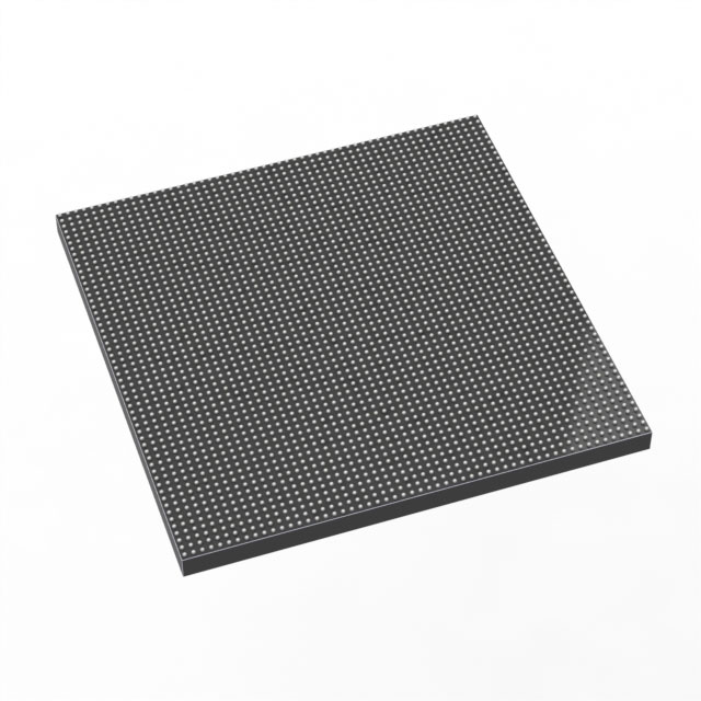
Overview of 1SG280HH2F55E2LGS3 – Stratix® 10 GX FPGA, 2,800,000 logic elements, 1160 I/Os, 2912-BBGA
The 1SG280HH2F55E2LGS3 is an Intel Stratix® 10 GX field programmable gate array (FPGA) in a 2912-ball FCBGA package, offered in Extended grade. It combines high logic capacity, large on-chip RAM, and extensive I/O to address advanced, bandwidth- and compute-intensive designs.
Built on Stratix 10 family innovations, this device targets high-performance applications that require dense logic, high-speed transceivers, and advanced DSP and memory resources while operating within a supply range of 820 mV to 880 mV and an ambient range of 0 °C to 100 °C.
Key Features
- Core Architecture Part of the Stratix 10 GX family, incorporating the Intel Hyperflex core architecture and 14 nm tri-gate (FinFET) process technologies cited for improved core performance.
- Logic Capacity Approximately 2,800,000 logic elements to implement large, complex digital designs.
- On-chip Memory Total RAM: 240,123,904 bits, with internal M20K memory block architecture referenced in the Stratix 10 family.
- I/O and Packaging 1160 user I/Os in a 2912-BBGA (55 × 55 mm FCBGA) surface-mount package, suited for dense board-level integration.
- High-speed Transceivers & Interfaces Stratix 10 family transceiver capabilities include multi-gigabit channels and transceiver data rates up to 28.3 Gbps, plus hard IP options such as PCI Express Gen3 x16 and 10G Ethernet FEC noted in the device family overview.
- DSP and Compute Family-level variable-precision DSP blocks support high-throughput signal processing; Stratix 10 family material references up to 10 TFLOP compute and power-efficiency characteristics for DSP resources.
- Power and Supply Specified core supply range of 820 mV to 880 mV for device operation.
- Operating Range & Grade Extended grade device with an operating temperature range of 0 °C to 100 °C.
- Compliance RoHS-compliant.
- Configuration & System Features Stratix 10 family documentation describes integrated features such as secure device management, configuration options, and SEU detection and correction mechanisms.
Typical Applications
- High-speed Networking and Switches Large logic capacity, high I/O count, and multi-gigabit transceiver performance make this device suitable for line cards, switches, and other networking infrastructure requiring high bandwidth.
- Data Center Accelerators Dense logic and significant DSP/memory resources support compute- and I/O-intensive acceleration tasks in data center environments.
- High-performance Signal Processing On-chip RAM and variable-precision DSP blocks enable complex signal-processing pipelines for communications and instrumentation.
- PCI Express-based Systems Support for hard PCI Express Gen3 x16 IP (noted in the family overview) allows implementation of high-throughput host interfaces and adapters.
Unique Advantages
- High Logic Density: Approximately 2.8 million logic elements allow integration of large, multi-function designs into a single FPGA package, reducing board-level complexity.
- Extensive On-chip Memory: 240,123,904 total RAM bits provide substantial embedded storage for buffering, data staging, and algorithmic state without external memory.
- Broad High-speed I/O: 1160 I/Os and family-level multi-gigabit transceivers enable flexible routing and direct connections to high-bandwidth peripherals and backplanes.
- Advanced Compute Fabric: Stratix 10 family DSP capabilities and Hyperflex core architecture support demanding signal-processing and compute workloads.
- Compact, Board-ready Package: 2912-ball FCBGA (55 × 55 mm) surface-mount package balances high pin count with manufacturability for dense system designs.
- Extended Grade Operation: Specified for 0 °C to 100 °C operation to match systems designed for extended commercial temperature environments.
Why Choose 1SG280HH2F55E2LGS3?
This Stratix® 10 GX FPGA delivers a combination of high logic capacity, large embedded RAM, extensive I/O, and the Stratix 10 family’s advanced architectural features for designs that demand both bandwidth and compute density. Its Extended grade rating and defined supply and temperature ranges make it suitable for systems that require robust performance within those environmental limits.
The device leverages documented Stratix 10 GX family innovations—such as the Hyperflex core architecture, high-speed transceivers, DSP resources, and hardened interface IP—to provide a platform that scales for complex networking, acceleration, and signal-processing designs while consolidating functions to reduce BOM and board complexity.
Request a quote or submit an inquiry to receive pricing, lead-time, and ordering information for the 1SG280HH2F55E2LGS3 Stratix® 10 GX FPGA.


Date Founded: 1968
Headquarters: Santa Clara, California, USA
Employees: 130,000+
Revenue: $54.23 Billion
Certifications and Memberships: ISO9001:2015, ISO14001:2015, ISO17025:2017, ISO27001:2022, ISO45001:2018, ISO50001:2018


