
1SG280HH3F55E1VGS3
| Part Description |
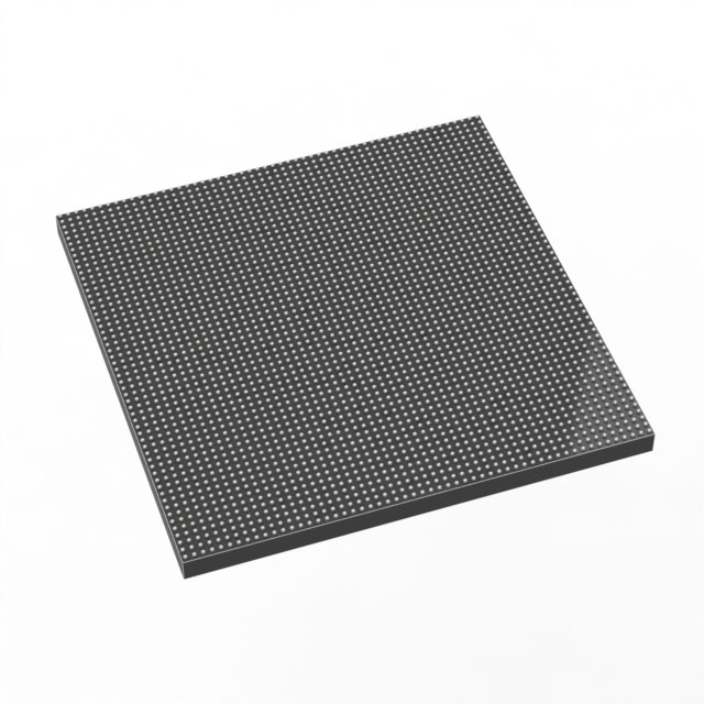
Stratix® 10 GX Field Programmable Gate Array (FPGA) IC 1160 2800000 2912-BBGA, FCBGA |
|---|---|
| Quantity | 642 Available (as of October 7, 2026) |
| Product Category | Field Programmable Gate Array (FPGA) |
|---|---|
| Manufacturer | Intel |
| Manufacturing Status | Active |
| Manufacturer Standard Lead Time | 9 Weeks |
| Datasheet |
Specifications & Environmental
| Device Package | 2912-FBGA, FC (55x55) | Grade | Extended | Operating Temperature | 0°C – 100°C | ||
|---|---|---|---|---|---|---|---|
| Package / Case | 2912-BBGA, FCBGA | Number of I/O | 1160 | Voltage | 770 mV - 970 mV | ||
| Mounting Method | Surface Mount | RoHS Compliance | Unknown | REACH Compliance | REACH Unaffected | ||
| Moisture Sensitivity Level | 3 (168 Hours) | Number of LABs/CLBs | 350000 | Number of Logic Elements/Cells | 2800000 | ||
| Number of Gates | N/A | ECCN | N/A | HTS Code | N/A | ||
| Qualification | N/A | Total RAM Bits | 240123904 |
Overview of 1SG280HH3F55E1VGS3 – Stratix® 10 GX FPGA, 2,800,000 logic elements, 2912-BBGA
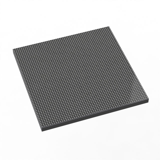
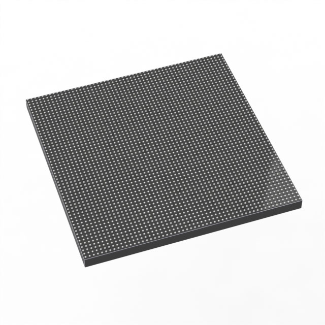
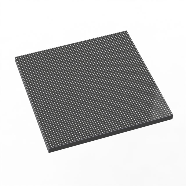
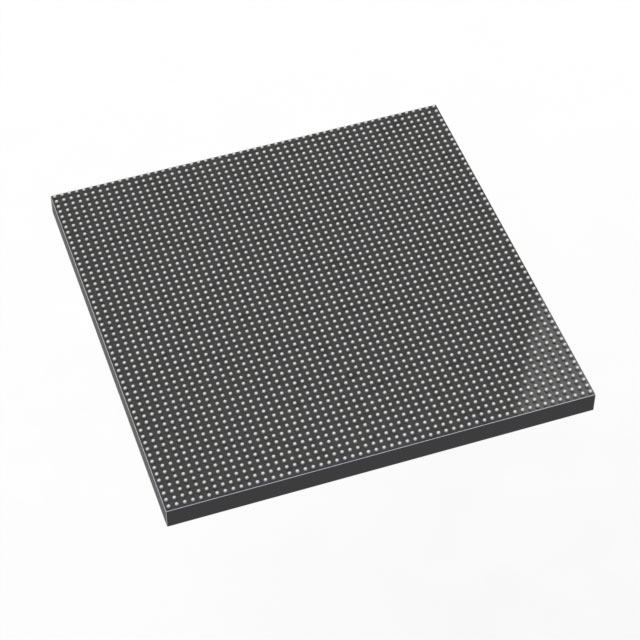
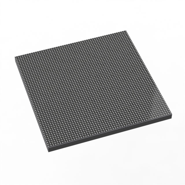
The 1SG280HH3F55E1VGS3 is an Intel Stratix® 10 GX field programmable gate array supplied in a 2912-ball FCBGA package (55×55). It pairs a high logic-element capacity with large on-chip RAM and extensive I/O to address advanced, high-throughput hardware designs.
As part of the Stratix 10 family, this device leverages the family’s core architecture and high-performance platform innovations to serve demanding applications that require dense logic, large embedded memory, and substantial I/O bandwidth while operating within a 0 °C to 100 °C range.
Key Features
- Core Architecture (family-level): Intel Hyperflex core architecture and 14 nm tri-gate technology are highlighted in the Stratix 10 family overview, supporting higher core performance and efficiency.
- Logic Density: 2,800,000 logic elements (logic element cells) for complex, high-density digital designs.
- Embedded Memory: 240,123,904 total RAM bits to store large datasets, buffers, and state for data-intensive processing.
- I/O Capacity: 1,160 user I/Os to support broad external interfacing and high-pin-count systems integration.
- Power Supply Range: Core voltage range of 770 mV to 970 mV to match system power design requirements.
- Package & Mounting: 2912-BBGA FCBGA (supplier package: 2912-FBGA, FC (55×55)); surface-mount mounting type for board-level assembly.
- Temperature Grade: Extended grade with an operating temperature range of 0 °C to 100 °C suitable for many industrial and commercial environments.
- Compliance: RoHS compliant.
- Family-Level I/O & Transceiver Capabilities: Stratix 10 family overview documents high-performance transceiver and interface features (for example, high-speed serial transceivers, PCI Express and Ethernet hard IP are described at the family level).
Typical Applications
- High‑Performance Networking: Implement network engines, packet processors, and line cards that require extensive logic, embedded memory, and many I/Os.
- Telecom & Data Center Infrastructure: Build backplane and switch fabrics leveraging the device’s high logic capacity and family-level transceiver capabilities for bandwidth-centric designs.
- Compute Acceleration: Deploy custom accelerators and data-path engines that use large on-chip RAM and dense logic to offload compute-intensive tasks.
- Advanced Prototyping and System Integration: Use the high I/O count and large logic/memory resources for complex SoC prototyping and heterogeneous system integration.
Unique Advantages
- High Logic Capacity: 2.8 million logic elements provide the resource headroom for large, complex FPGA designs without partitioning across multiple devices.
- Substantial On‑Chip Memory: Over 240 million RAM bits enable deep buffering, large lookup tables, and data staging within the FPGA fabric.
- Extensive I/O Reach: 1,160 I/Os allow flexible connectivity to high-pin-count peripherals, memory interfaces, and board-level interconnects.
- Robust Thermal and Power Envelope: Extended temperature grade (0 °C to 100 °C) and defined core voltage range (770 mV–970 mV) simplify system power and thermal planning.
- Industry‑Compliant Packaging: 2912-ball FCBGA (55×55) surface-mount package supports modern PCB assembly processes for high-density boards.
- Backed by Stratix 10 Family Innovations: Family-level features such as the Hyperflex core architecture and advanced transceiver/IP options offer a platform designed for high throughput and efficiency.
Why Choose 1SG280HH3F55E1VGS3?
The 1SG280HH3F55E1VGS3 positions itself as a high-capacity Stratix 10 GX FPGA option for designs that demand large logic resources, significant embedded RAM, and a high I/O count in a 2912-ball FCBGA package. It is suitable for engineers building bandwidth- and compute-intensive systems where on-chip resources and robust interfacing are critical.
Choosing this device provides access to the Stratix 10 family’s architectural advancements while delivering a defined operating range and RoHS compliance—making it a practical choice for long-lived, scalable hardware designs that leverage a high-performance FPGA platform.
If you would like availability, pricing, or a formal quote for 1SG280HH3F55E1VGS3, request a quote or submit an inquiry and our team will respond with the information you need.





















Date Founded: 1968
Headquarters: Santa Clara, California, USA
Employees: 130,000+
Revenue: $54.23 Billion
Certifications and Memberships: ISO9001:2015, ISO14001:2015, ISO17025:2017, ISO27001:2022, ISO45001:2018, ISO50001:2018


