
1SG280HN2F43E2LG
| Part Description |
Stratix® 10 GX Field Programmable Gate Array (FPGA) IC 688 2800000 1760-BBGA, FCBGA |
|---|---|
| Quantity | 1,281 Available (as of October 7, 2026) |
| Product Category | Field Programmable Gate Array (FPGA) |
|---|---|
| Manufacturer | Intel |
| Manufacturing Status | Active |
| Manufacturer Standard Lead Time | 12 Weeks |
| Datasheet |
Specifications & Environmental
| Device Package | 1760-FBGA (42.5x42.5) | Grade | Extended | Operating Temperature | 0°C – 100°C | ||
|---|---|---|---|---|---|---|---|
| Package / Case | 1760-BBGA, FCBGA | Number of I/O | 688 | Voltage | 820 mV - 880 mV | ||
| Mounting Method | Surface Mount | RoHS Compliance | Unknown | REACH Compliance | REACH Unaffected | ||
| Moisture Sensitivity Level | 3 (168 Hours) | Number of LABs/CLBs | 350000 | Number of Logic Elements/Cells | 2800000 | ||
| Number of Gates | N/A | ECCN | N/A | HTS Code | N/A | ||
| Qualification | N/A | Total RAM Bits | 240123904 |
Overview of 1SG280HN2F43E2LG – Stratix® 10 GX FPGA, 1760‑BBGA
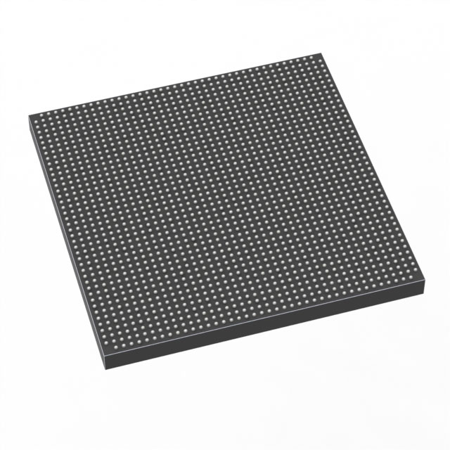
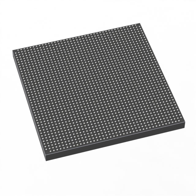
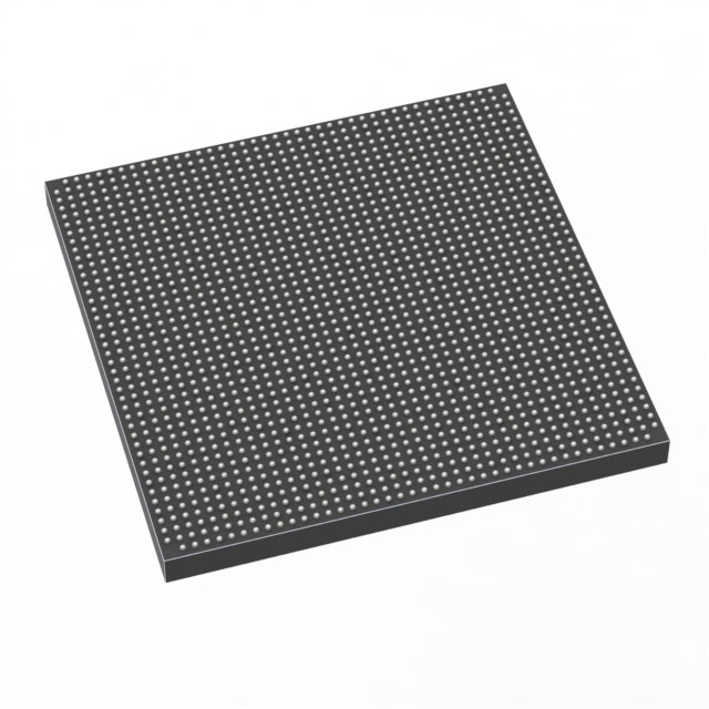
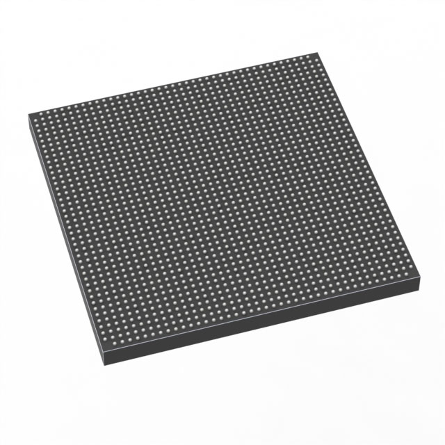
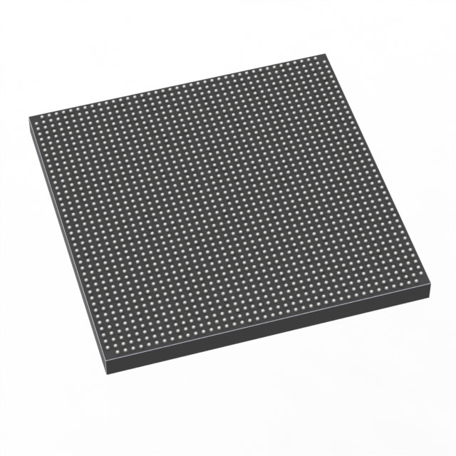
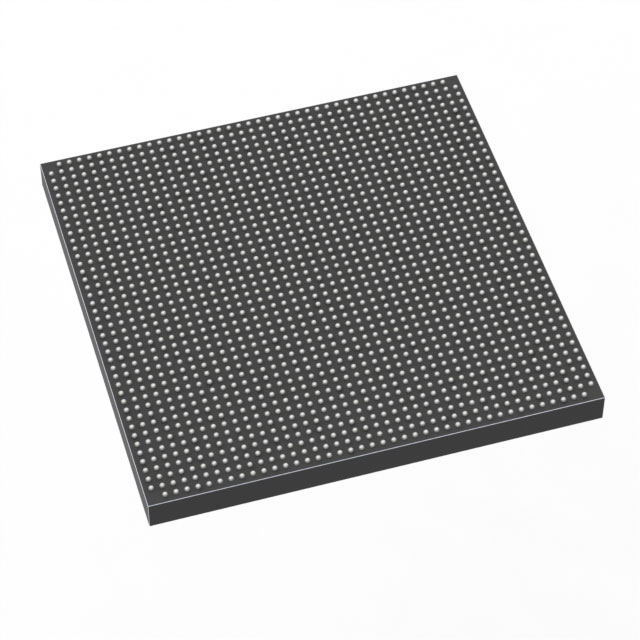
The 1SG280HN2F43E2LG is an Intel Stratix® 10 GX field‑programmable gate array delivered in a 1760‑ball FCBGA (42.5 × 42.5 mm) package. Built on the Stratix® 10 GX family architecture, it leverages the Hyperflex core architecture and Intel 14 nm tri‑gate (FinFET) technology to address advanced, high‑performance programmable logic requirements.
This device targets applications that require large programmable fabric, substantial on‑chip memory, and high I/O density—providing designers with a platform for bandwidth‑ and compute‑intensive systems while meeting extended‑grade environmental requirements.
Key Features
- Core Logic 2,800,000 logic elements (LEs) for high-capacity programmable logic integration.
- Memory 240,123,904 total RAM bits of on‑chip memory to support large buffering, lookup tables, and local data storage.
- I/O Density 688 user I/O pins to accommodate wide parallel interfaces and high‑pin‑count peripherals.
- Package & Mounting 1760‑BBGA (FCBGA) supplier device package, 1760‑FBGA (42.5 × 42.5 mm); surface‑mount package optimized for board‑level assembly.
- Power Supply Core voltage range of 820 mV to 880 mV for the device core supply rails.
- Operating Temperature & Grade Extended grade with an operating range of 0 °C to 100 °C for deployment in higher temperature environments within the extended specification window.
- Standards & Compliance RoHS compliant for adherence to common environmental regulations.
- Family Innovations (Stratix® 10) Family features include the Intel Hyperflex core architecture and Intel 14 nm tri‑gate (FinFET) technology as described in the Stratix® 10 GX device overview.
Typical Applications
- High‑Bandwidth Networking Large logic capacity and high I/O count support packet processing, switch/router functions, and advanced interface bridging.
- Data Center Acceleration Substantial on‑chip RAM and logic resources enable custom acceleration kernels and dataflow engines for compute‑intensive workloads.
- Communications & Transport The Stratix® 10 family’s architecture targets systems that require high processing performance and flexible protocol implementation.
- Advanced Signal Processing Large fabric and memory resources support complex digital signal processing pipelines and buffering for high‑throughput signal chains.
Unique Advantages
- High Logic Capacity: 2.8 million logic elements enable large, highly parallel designs and consolidation of multiple functions into a single device.
- Large On‑Chip Memory: Over 240 million bits of RAM provide the headroom needed for deep buffering, large LUTs, and state storage without immediate external memory dependence.
- High I/O Count: 688 I/O pins allow wide parallel interfaces and multiple concurrent peripheral connections, reducing the need for external multiplexing.
- Modern Process & Architecture: Leveraging Intel 14 nm tri‑gate (FinFET) process and the Hyperflex core architecture (as detailed for Stratix® 10 GX devices) for improved core performance per the family overview.
- Extended Operating Grade: Rated for 0 °C to 100 °C operation and supplied in a surface‑mount FCBGA package suitable for dense board implementations.
- Regulatory Compliance: RoHS compliance supports integration into products requiring this environmental conformance.
Why Choose 1SG280HN2F43E2LG?
The 1SG280HN2F43E2LG brings large‑scale programmable logic, extensive on‑chip memory, and high pin density in a single FCBGA package—positioning it for designs that demand significant compute and data buffering close to the fabric. As part of the Stratix® 10 GX family, it benefits from the family’s core architectural improvements and process technologies described in the device overview.
This device is well suited to engineers building bandwidth‑ and computation‑heavy systems that require scalable FPGA fabric and robust I/O. Its combination of logic capacity, memory resources, and extended‑grade operation provides long‑term value for advanced communication, data center, and signal processing projects.
Request a quote or submit a quote for part number 1SG280HN2F43E2LG to receive pricing and lead‑time information for your procurement and design planning.





















Date Founded: 1968
Headquarters: Santa Clara, California, USA
Employees: 130,000+
Revenue: $54.23 Billion
Certifications and Memberships: ISO9001:2015, ISO14001:2015, ISO17025:2017, ISO27001:2022, ISO45001:2018, ISO50001:2018


