
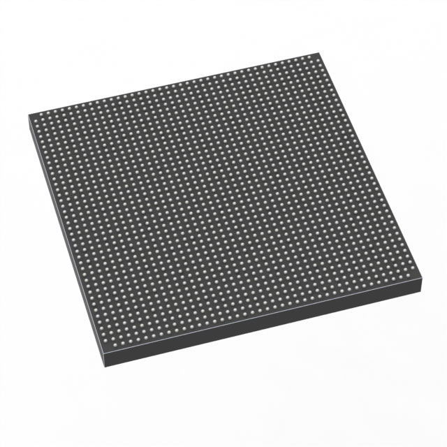
1SG280HN2F43E2LGS3
| Part Description |
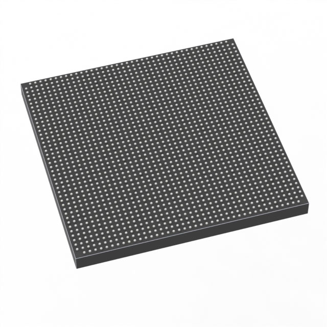
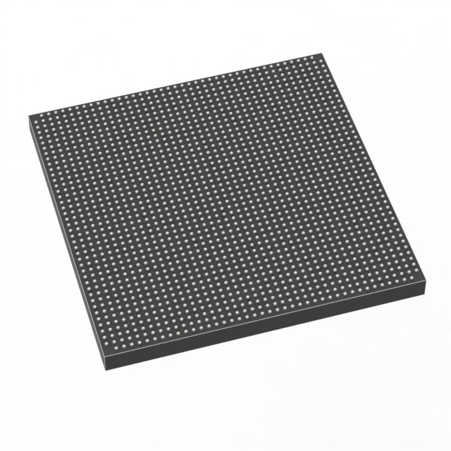
Stratix® 10 GX Field Programmable Gate Array (FPGA) IC 688 2800000 1760-BBGA, FCBGA |
|---|---|
| Quantity | 1,133 Available (as of October 8, 2026) |
| Product Category | Field Programmable Gate Array (FPGA) |
|---|---|
| Manufacturer | Intel |
| Manufacturing Status | Active |
| Manufacturer Standard Lead Time | 8 Weeks |
| Datasheet |
Specifications & Environmental
| Device Package | 1760-FBGA (42.5x42.5) | Grade | Extended | Operating Temperature | 0°C – 100°C | ||
|---|---|---|---|---|---|---|---|
| Package / Case | 1760-BBGA, FCBGA | Number of I/O | 688 | Voltage | 820 mV - 880 mV | ||
| Mounting Method | Surface Mount | RoHS Compliance | Unknown | REACH Compliance | REACH Unaffected | ||
| Moisture Sensitivity Level | 3 (168 Hours) | Number of LABs/CLBs | 350000 | Number of Logic Elements/Cells | 2800000 | ||
| Number of Gates | N/A | ECCN | N/A | HTS Code | N/A | ||
| Qualification | N/A | Total RAM Bits | 240123904 |
Overview of 1SG280HN2F43E2LGS3 – Stratix® 10 GX FPGA IC, 2,800,000 Logic Elements, 1760-BBGA
The 1SG280HN2F43E2LGS3 is an Intel Stratix® 10 GX field programmable gate array (FPGA) in a 1760-ball FCBGA package. It combines a high-capacity programmable fabric with on-chip memory and high-density I/O to address demanding bandwidth and compute requirements.
Built on the Stratix 10 GX family architecture, the device leverages the Hyperflex core innovations and advanced transceiver capabilities to deliver increased core performance and energy-efficient processing for advanced communications, networking, and compute-accelerated designs.
Key Features
- Core architecture Hyperflex-based Stratix 10 GX family architecture as described in the device overview, providing higher core performance compared to previous generation high-performance FPGAs.
- Logic capacity 2,800,000 logic elements suitable for large-scale, complex digital designs.
- On-chip memory 240,123,904 total RAM bits (device total internal memory), with family memory architectures including M20K internal SRAM blocks referenced in the device overview.
- I/O and transceivers 688 general-purpose I/O pins and family-level transceiver capabilities designed for high-speed serial links; the Stratix 10 GX family overview documents high-speed transceiver technology for demanding I/O applications.
- High-speed interfaces (family features) Stratix 10 GX family-level hard IP and transceiver features include PCI Express Gen3 support, 10G Ethernet FEC in transceiver channels, and support for high-rate DDR4 memory PHYs (as noted in the device overview).
- Process and performance Part of the 14 nm Stratix 10 family with architecture-level improvements delivering higher performance and improved power efficiency over prior high-performance FPGA generations (family overview).
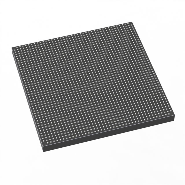
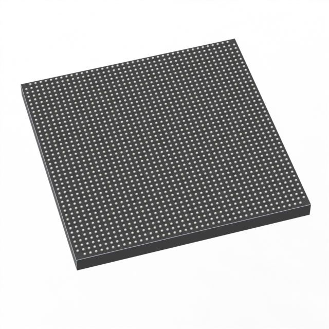
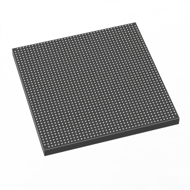
- Package and mounting 1760-BBGA (FCBGA) surface-mount package, supplier device package 1760-FBGA with 42.5 × 42.5 mm body size.
- Power and supply Core voltage supply range: 820 mV to 880 mV.
- Operating range and grade Extended grade device with an operating temperature range of 0 °C to 100 °C and RoHS compliance.
Typical Applications
- High-performance networking and telecom Use the device for bandwidth- and latency-sensitive tasks thanks to the Stratix 10 GX family transceiver and hard IP features described in the device overview.
- Data center acceleration Large logic and on-chip memory capacity make this FPGA suitable for accelerator and offload functions that require significant programmable fabric and memory resources.
- High-speed compute and DSP Stratix 10 family DSP and compute capabilities support signal processing and compute-intensive workloads requiring substantial arithmetic throughput and precision.
- Backplane and module I/O Extensive I/O count and family transceiver technology enable integration into high-density module and backplane designs.
Unique Advantages
- Large programmable fabric: 2.8 million logic elements support complex, system-level FPGA implementations without partitioning across multiple devices.
- Substantial on-chip memory: Over 240 million bits of internal RAM reduce reliance on external memory for many buffering and scratchpad needs.
- High-density I/O: 688 I/O pins provide broad peripheral and interface connectivity for mixed-signal and multi-protocol designs.
- Advanced package and thermal allowance: 1760-BBGA packaging in a 42.5 × 42.5 mm footprint with an operating range to 100 °C supports compact, high-density board designs.
- Family-level high-speed interface support: Stratix 10 GX family features include hardened interfaces and transceiver capabilities for PCIe, Ethernet, and high-speed memory PHYs as documented in the device overview.
- Energy-conscious core operation: Family-level architectural and process advancements target improved performance-per-watt compared with previous high-performance FPGA generations.
Why Choose 1SG280HN2F43E2LGS3?
The 1SG280HN2F43E2LGS3 positions designers to implement large, performance-focused FPGA systems by combining multi-million logic-element capacity, extensive on-chip RAM, and high-density I/O in a single Stratix 10 GX device. Its package, voltage range, and extended-grade operating temperature make it suitable for compact, high-density board layouts that require sustained performance up to 100 °C.
As part of the Intel Stratix 10 GX family, this device benefits from a platform of advanced architecture and high-speed interface options documented in the device overview, making it appropriate for teams tackling demanding networking, compute acceleration, and high-throughput I/O challenges while leveraging the Stratix ecosystem and documentation.
Request a quote or submit an inquiry to obtain pricing, availability, and lead-time details for the 1SG280HN2F43E2LGS3.





















Date Founded: 1968
Headquarters: Santa Clara, California, USA
Employees: 130,000+
Revenue: $54.23 Billion
Certifications and Memberships: ISO9001:2015, ISO14001:2015, ISO17025:2017, ISO27001:2022, ISO45001:2018, ISO50001:2018


