
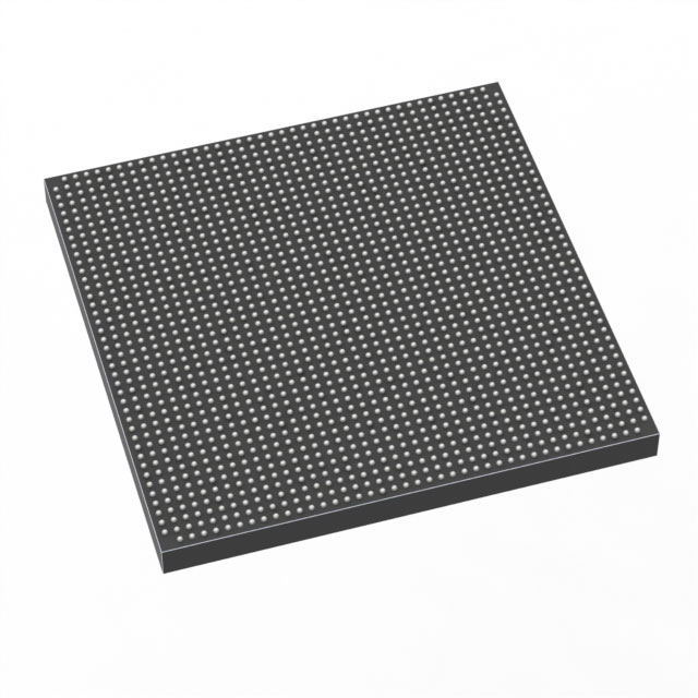
1SG280HN2F43E2VGAS
| Part Description |
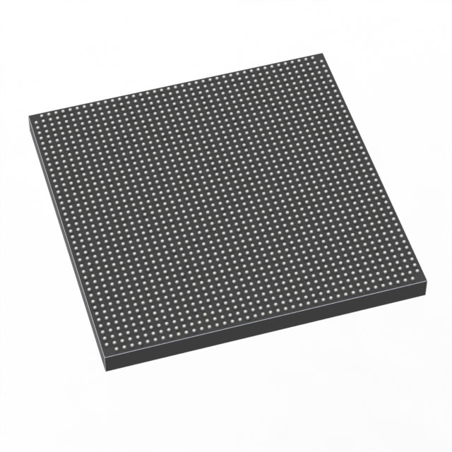
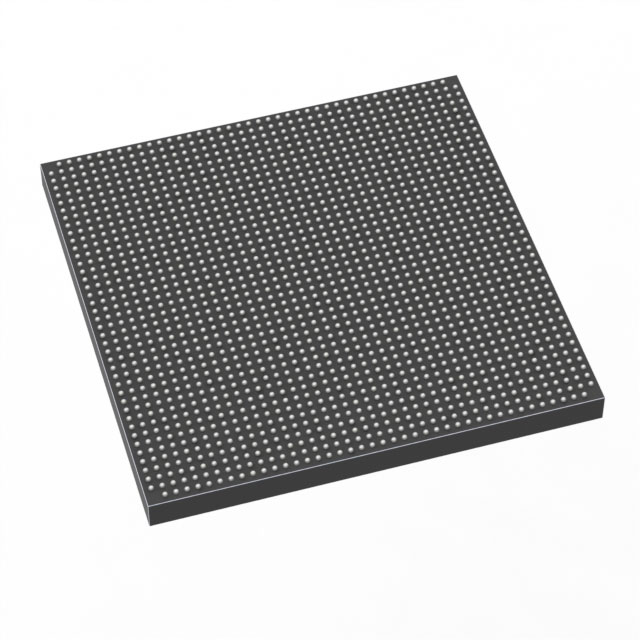
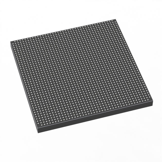
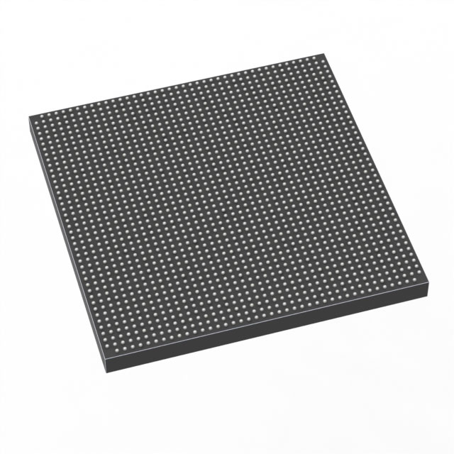
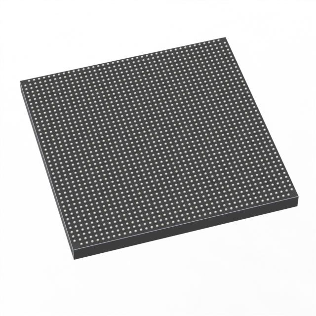
Stratix® 10 GX Field Programmable Gate Array (FPGA) IC 688 2800000 1760-BBGA, FCBGA |
|---|---|
| Quantity | 620 Available (as of October 7, 2026) |
| Product Category | Field Programmable Gate Array (FPGA) |
|---|---|
| Manufacturer | Intel |
| Manufacturing Status | Active |
| Manufacturer Standard Lead Time | 12 Weeks |
| Datasheet |
Specifications & Environmental
| Device Package | 1760-FBGA (42.5x42.5) | Grade | Extended | Operating Temperature | 0°C – 100°C | ||
|---|---|---|---|---|---|---|---|
| Package / Case | 1760-BBGA, FCBGA | Number of I/O | 688 | Voltage | 770 mV - 970 mV | ||
| Mounting Method | Surface Mount | RoHS Compliance | Unknown | REACH Compliance | REACH Unaffected | ||
| Moisture Sensitivity Level | 3 (168 Hours) | Number of LABs/CLBs | 350000 | Number of Logic Elements/Cells | 2800000 | ||
| Number of Gates | N/A | ECCN | N/A | HTS Code | N/A | ||
| Qualification | N/A | Total RAM Bits | 240123904 |
Overview of 1SG280HN2F43E2VGAS – Stratix® 10 GX Field Programmable Gate Array (FPGA) IC, 1760-BBGA
The 1SG280HN2F43E2VGAS is a Stratix® 10 GX family FPGA in a 1760-BBGA (FCBGA) package, designed for advanced applications that demand high logic density, large on-chip memory, and extensive I/O. Built on the Stratix 10 GX/SX device family architecture, the device incorporates the family’s Hyperflex core innovations and other Stratix 10 capabilities to address high-bandwidth, high-performance processing needs.
This device targets designs requiring millions of logic elements, substantial RAM, and high-speed interfacing while offering an extended operational grade and surface-mount package suitable for production deployments.
Key Features
- Logic Capacity — 2,800,000 logic elements (LEs) for dense logic implementation and large-scale FPGA designs.
- On-Chip Memory — 240,123,904 total RAM bits to support large buffering, packet processing, and state storage on-chip.
- I/O — 688 user I/O pins to enable extensive peripheral and high-speed interface connectivity.
- Power Supply — Core voltage supply range 770 mV to 970 mV.
- Package & Mounting — 1760-BBGA (FCBGA) package, supplier device package 1760-FBGA (42.5 × 42.5 mm); surface mount mounting type.
- Operating Range & Grade — Extended grade with operating temperature 0 °C to 100 °C; RoHS compliant.
- Family-Level Architecture — Stratix 10 family innovations including the Intel Hyperflex™ core architecture delivering improved core performance and power efficiency, and Intel 14 nm tri-gate (FinFET) process technology (family-level features documented in the Stratix 10 overview).
- High-Speed Transceiver and IP (Family-Level) — Family documentation cites heterogeneous 3D SiP transceiver tiles, transceiver data rates up to 28.3 Gbps, hard PCI Express Gen3 x16 IP, DDR4 memory controller support up to 2666 Mbps per pin, and advanced DSP blocks (family-level capabilities referenced in the device overview).
Typical Applications
- High-performance processing — On-chip memory and 2.8M logic elements support compute- and data-intensive hardware acceleration and FPGA-based processing engines.
- Networking and data transport — Large I/O count and family-level high-speed transceiver/PCIe capabilities suit high-bandwidth packet processing, switching, and network fabric applications.
- Digital signal processing — Extensive RAM and logic capacity enable complex DSP pipelines and variable-precision DSP implementations (family-level DSP resources documented in the Stratix 10 overview).
- Module and board-level integration — 1760-BBGA surface-mount package and abundant I/O make the device suitable for dense board designs requiring high integration.
Unique Advantages
- High logic density: 2,800,000 logic elements provide the capacity to implement large, complex designs without partitioning across multiple devices.
- Substantial on-chip memory: 240,123,904 total RAM bits reduce external memory dependence and improve throughput for buffering and stateful processing.
- Extensive I/O and packaging: 688 I/O pins in a 1760-BBGA (42.5 × 42.5 mm) surface-mount package support high-pin-count interfaces in a compact footprint.
- Designed for performance and efficiency (family-level): Stratix 10 family innovations such as the Hyperflex core architecture and 14 nm FinFET process yield higher core performance and improved power characteristics as documented in the device overview.
- High-speed interface support (family-level): Family documentation includes support for multi-gigabit transceivers, PCIe Gen3 hard IP, and high-rate DDR4 memory interfaces to streamline system-level integration.
- Production-ready grade and compliance: Extended grade rating, RoHS compliance, and standard surface-mount packaging support production deployments with defined temperature and supply ranges.
Why Choose 1SG280HN2F43E2VGAS?
The 1SG280HN2F43E2VGAS combines very high logic density, large on-chip memory, and extensive I/O in a production-friendly 1760-BBGA package, offering a platform for demanding FPGA designs that require significant compute and buffering on a single device. As part of the Stratix 10 GX family, it benefits from the documented family innovations—architectural and transceiver/IP capabilities—that address high-bandwidth and high-performance application needs.
This device is well suited to customers designing advanced processing, networking, and signal-processing systems who need a scalable, high-capacity FPGA with defined electrical and thermal operating ranges and industry-standard packaging for board-level integration.
Request a quote or submit an inquiry to receive pricing and availability information for 1SG280HN2F43E2VGAS.





















Date Founded: 1968
Headquarters: Santa Clara, California, USA
Employees: 130,000+
Revenue: $54.23 Billion
Certifications and Memberships: ISO9001:2015, ISO14001:2015, ISO17025:2017, ISO27001:2022, ISO45001:2018, ISO50001:2018


