
1SG280HN2F43I2LG
| Part Description |
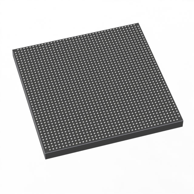
Stratix® 10 GX Field Programmable Gate Array (FPGA) IC 688 2800000 1760-BBGA, FCBGA |
|---|---|
| Quantity | 443 Available (as of June 15, 2026) |

| Product Category | Field Programmable Gate Array (FPGA) |
|---|---|
| Manufacturer | Intel |
| Manufacturing Status | Active |
| Manufacturer Standard Lead Time | 12 Weeks |
| Datasheet |
Specifications & Environmental
| Device Package | 1760-FBGA (42.5x42.5) | Grade | Industrial | Operating Temperature | -40°C – 100°C | ||
|---|---|---|---|---|---|---|---|
| Package / Case | 1760-BBGA, FCBGA | Number of I/O | 688 | Voltage | 820 mV - 880 mV | ||
| Mounting Method | Surface Mount | RoHS Compliance | Unknown | REACH Compliance | REACH Unaffected | ||
| Moisture Sensitivity Level | 3 (168 Hours) | Number of LABs/CLBs | 350000 | Number of Logic Elements/Cells | 2800000 | ||
| Number of Gates | N/A | ECCN | N/A | HTS Code | N/A | ||
| Qualification | N/A | Total RAM Bits | 240123904 |
Overview of 1SG280HN2F43I2LG – Stratix® 10 GX FPGA, 1760-BBGA
The 1SG280HN2F43I2LG is an Intel Stratix® 10 GX field programmable gate array (FPGA) in a 1760-BBGA FCBGA package. Built on the Stratix 10 GX family architecture, it targets advanced designs that require high logic density, extensive embedded memory, and substantial I/O capability.
This device is suited for high-bandwidth, compute-intensive applications where substantial on-chip RAM, large numbers of logic elements, and robust I/O are required. Its core architecture and package characteristics support demanding industrial applications across networking, data processing, and communications equipment.
Key Features
- Core Logic — 2,800,000 logic elements (cells) provide significant programmable fabric for complex digital designs.
- Embedded Memory — 240,123,904 total RAM bits for large on-chip buffering, lookup tables, and data structures.
- I/O Density — 688 general purpose I/O pins to support wide parallel interfaces and high-pin-count connectivity.
- Transceiver & High-Speed Features — Stratix 10 GX series innovations include high-performance transceiver technology and advanced core architecture referenced in the device overview.
- Package & Mounting — 1760-BBGA (FCBGA) supplier device package 1760-FBGA (42.5 × 42.5 mm), surface-mount for compact board integration.
- Power — Core voltage supply specified from 820 mV to 880 mV, enabling tightly controlled power domains.
- Operating Temperature — Industrial-grade operating range from −40°C to 100°C for deployment in thermally demanding environments.
- Compliance — RoHS compliant.
Typical Applications
- Network Infrastructure — Implement high-throughput packet processing, traffic management, and protocol acceleration using the device's large logic capacity and abundant I/O.
- Data Center Acceleration — Offload compute-intensive functions and inline data processing where significant on-chip RAM and logic resources reduce latency and external memory dependence.
- Telecommunications Equipment — Support line cards, backplane interfaces, and aggregation systems that require dense I/O and high-performance programmable logic.
- Test & Measurement Systems — Use the device for real-time signal processing, data capture, and custom instrumentation requiring large memory and programmable compute.
Unique Advantages
- High Logic Density: 2.8 million logic elements enable complex algorithms and large-scale custom architectures on a single device.
- Large On-Chip Memory: 240,123,904 RAM bits reduce reliance on external memory and improve deterministic performance for buffering and state storage.
- Extensive I/O Footprint: 688 I/O pins provide the flexibility to interface with multiple parallel buses, high-pin-count connectors, and mixed-signal front ends.
- Industrial Temperature Range: Rated from −40°C to 100°C to meet thermal demands of industrial deployments.
- Compact, High-Pin Package: 1760-BBGA (42.5 × 42.5 mm) delivers high connectivity in a board-friendly form factor suitable for dense system designs.
- Controlled Core Voltage: 820–880 mV supply specification supports optimized power architecture and predictable power budgeting.
Why Choose 1SG280HN2F43I2LG?
1SG280HN2F43I2LG positions itself as a high-density Stratix 10 GX FPGA option for engineers designing bandwidth- and compute-focused systems. With millions of logic elements, hundreds of megabits of on-chip RAM, and extensive I/O, it supports sophisticated architectures that consolidate functionality and reduce external component count.
Engineers and procurement teams building networking, data center acceleration, telecommunications, or advanced industrial systems will find this device offers the integration and thermal range needed for robust, long-lived deployments, backed by the Stratix 10 family technical foundations documented in the device overview.
Request a quote or submit a pricing and availability inquiry to begin integrating the 1SG280HN2F43I2LG into your next design.


Date Founded: 1968
Headquarters: Santa Clara, California, USA
Employees: 130,000+
Revenue: $54.23 Billion
Certifications and Memberships: ISO9001:2015, ISO14001:2015, ISO17025:2017, ISO27001:2022, ISO45001:2018, ISO50001:2018


