
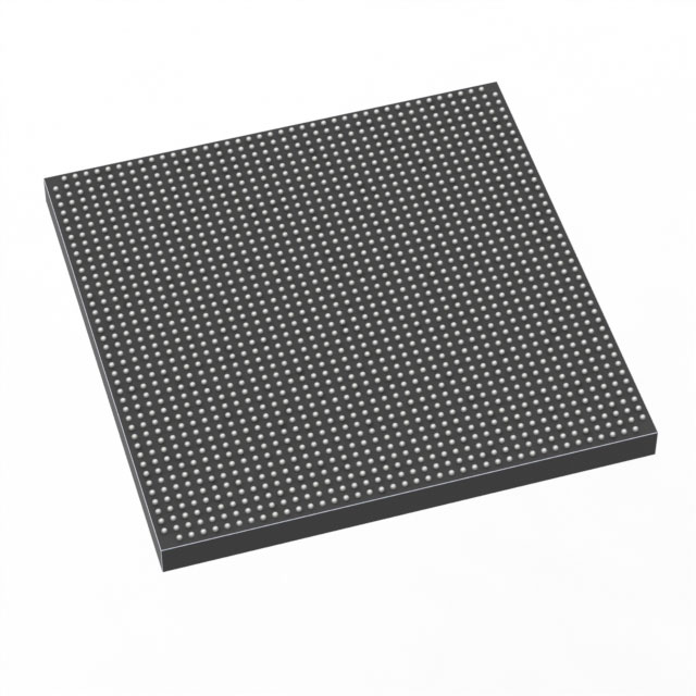
1SG280HN3F43E1VG
| Part Description |
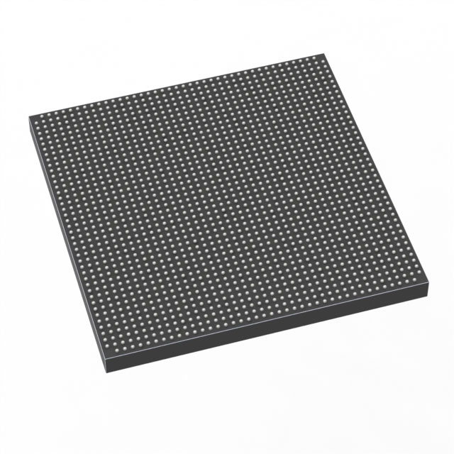
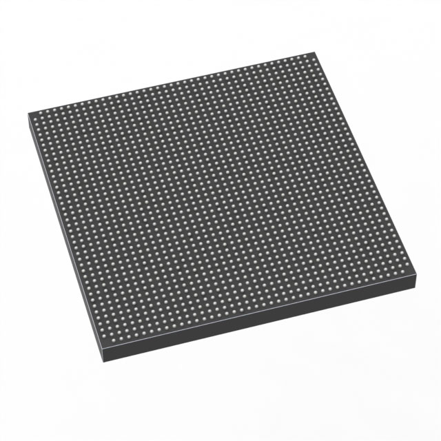
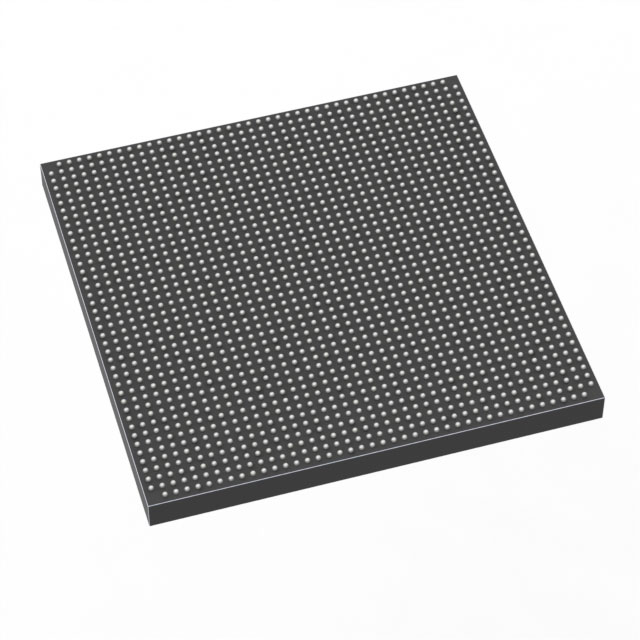
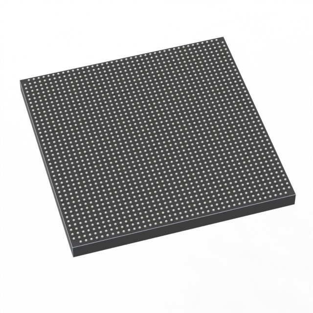
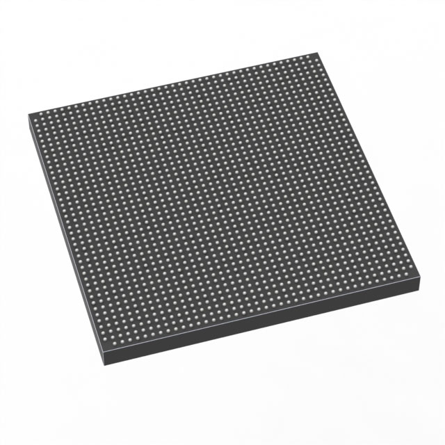
Stratix® 10 GX Field Programmable Gate Array (FPGA) IC 688 2800000 1760-BBGA, FCBGA |
|---|---|
| Quantity | 644 Available (as of October 8, 2026) |
| Product Category | Field Programmable Gate Array (FPGA) |
|---|---|
| Manufacturer | Intel |
| Manufacturing Status | Active |
| Manufacturer Standard Lead Time | 12 Weeks |
| Datasheet |
Specifications & Environmental
| Device Package | 1760-FBGA (42.5x42.5) | Grade | Extended | Operating Temperature | 0°C – 100°C | ||
|---|---|---|---|---|---|---|---|
| Package / Case | 1760-BBGA, FCBGA | Number of I/O | 688 | Voltage | 770 mV - 970 mV | ||
| Mounting Method | Surface Mount | RoHS Compliance | Unknown | REACH Compliance | REACH Unaffected | ||
| Moisture Sensitivity Level | 3 (168 Hours) | Number of LABs/CLBs | 350000 | Number of Logic Elements/Cells | 2800000 | ||
| Number of Gates | N/A | ECCN | N/A | HTS Code | N/A | ||
| Qualification | N/A | Total RAM Bits | 240123904 |
Overview of 1SG280HN3F43E1VG – Stratix® 10 GX FPGA, 1760‑BBGA (42.5×42.5), 688 I/O
The 1SG280HN3F43E1VG is an Intel Stratix® 10 GX field programmable gate array (FPGA) supplied in a 1760‑BBGA FCBGA package (1760‑FBGA, 42.5×42.5). It integrates a high‑density programmable fabric targeted at high‑performance applications that require large logic capacity, extensive on‑chip memory, and a broad complement of I/O.
Built around the Stratix 10 family architecture, this device leverages the family’s advanced core innovations to deliver increased on‑chip processing capability and efficient power use for demanding communications, compute acceleration, and advanced networking designs.
Key Features
- Logic Capacity — 2,800,000 logic elements, providing a high density of programmable logic for complex designs and large-scale integration.
- Embedded Memory — 240,123,904 total RAM bits to support large buffering, on‑chip storage, and memory‑intensive processing tasks.
- I/O Resources — 688 I/O pins to accommodate wide external interfaces, parallel buses, and multi‑lane connectivity.
- Core Architecture — Devices in the Stratix 10 family incorporate the Intel Hyperflex core architecture to increase core performance and efficiency for compute‑heavy workloads.
- Package and Mounting — 1760‑BBGA, FCBGA package (supplier device package: 1760‑FBGA, 42.5×42.5) in a surface‑mount form factor for system board integration.
- Power Supply — Core voltage range from 770 mV to 970 mV, enabling optimized power domain design and supply selection.
- Operating Range & Grade — Extended grade with an operating temperature range of 0°C to 100°C suitable for many commercial and enterprise environments.
- Compliance — RoHS compliant, supporting regulatory and environmental requirements for lead‑free assembly.
Typical Applications
- High‑Performance Networking — Use the device’s large logic count, extensive on‑chip memory, and large I/O complement for packet processing, switching fabrics, and interface bridging in networking equipment.
- Data Center Acceleration — Leverage the high logic and memory resources for compute acceleration, offload engines, and custom IP for latency‑sensitive workloads.
- Telecommunications Infrastructure — Deploy in systems that require large programmable fabric and numerous I/O for line cards, backplane interfaces, and protocol processing.
- Test, Measurement, and Prototyping — Implement complex signal processing and system emulation that demand substantial on‑chip RAM and programmable logic.
Unique Advantages
- High Logic Density: 2.8 million logic elements enable consolidation of large, multi‑function designs into a single device, reducing BOM and board complexity.
- Large On‑Chip Memory: 240,123,904 total RAM bits provide ample storage for buffering, lookup tables, and state retention without relying exclusively on external memory.
- Broad I/O Count: 688 I/O pins support diverse external interfaces and wide parallel connections, simplifying system integration for multi‑lane applications.
- Stratix 10 Family Innovations: Family features such as the Hyperflex core architecture provide documented improvements in core performance and efficient implementation of compute‑intensive functions.
- Packaged for System Integration: The 1760‑FBGA 42.5×42.5 package in a surface‑mount footprint facilitates dense placement on modern PCBs and standard assembly flows.
- Compliance and Grade: RoHS compliance and extended temperature grading support enterprise and commercial deployments with regulatory and environmental considerations addressed.
Why Choose 1SG280HN3F43E1VG?
The 1SG280HN3F43E1VG positions itself where large programmable capacity, significant on‑chip memory, and extensive I/O are required. Its Stratix 10 GX family heritage and Hyperflex architectural elements provide a platform suitable for demanding processing, networking, and acceleration tasks while enabling designers to consolidate functionality and manage board‑level complexity.
This device is a fit for teams developing complex FPGA‑centric systems that need a balance of logic density, memory resources, and a broad external interface set, offering scalability within Stratix 10 family device characteristics and vendor ecosystem support.
Request a quote or submit an inquiry to obtain pricing, availability, and lead‑time information for the 1SG280HN3F43E1VG. Our team will provide the details needed to move your design forward.





















Date Founded: 1968
Headquarters: Santa Clara, California, USA
Employees: 130,000+
Revenue: $54.23 Billion
Certifications and Memberships: ISO9001:2015, ISO14001:2015, ISO17025:2017, ISO27001:2022, ISO45001:2018, ISO50001:2018


