
1SG280HN3F43E1VGS3
| Part Description |
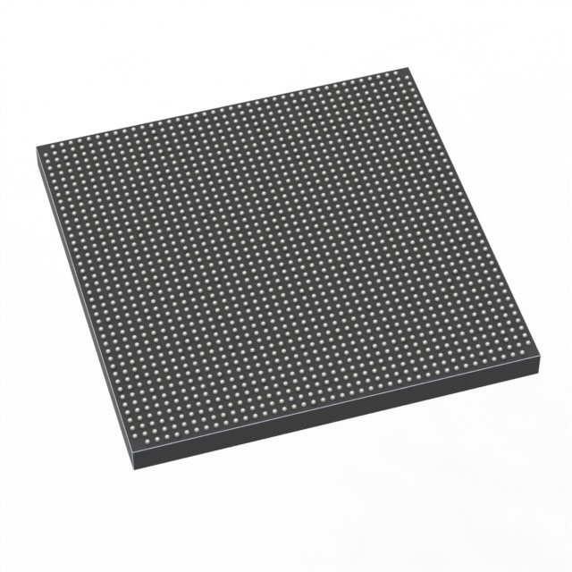
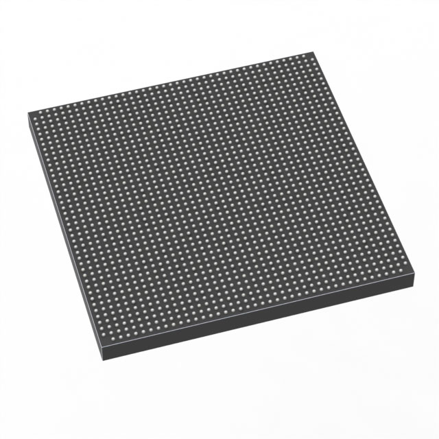
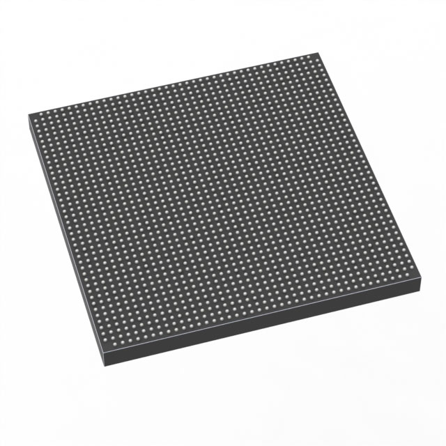
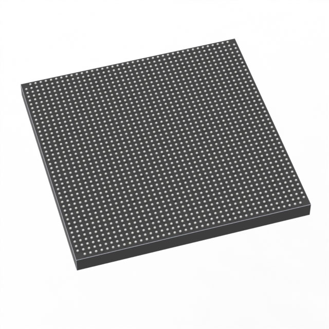
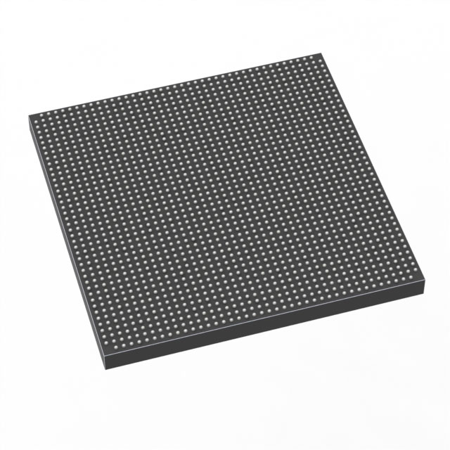
Stratix® 10 GX Field Programmable Gate Array (FPGA) IC 688 2800000 1760-BBGA, FCBGA |
|---|---|
| Quantity | 1,041 Available (as of October 7, 2026) |
| Product Category | Field Programmable Gate Array (FPGA) |
|---|---|
| Manufacturer | Intel |
| Manufacturing Status | Active |
| Manufacturer Standard Lead Time | 8 Weeks |
| Datasheet |
Specifications & Environmental
| Device Package | 1760-FBGA (42.5x42.5) | Grade | Extended | Operating Temperature | 0°C – 100°C | ||
|---|---|---|---|---|---|---|---|
| Package / Case | 1760-BBGA, FCBGA | Number of I/O | 688 | Voltage | 770 mV - 970 mV | ||
| Mounting Method | Surface Mount | RoHS Compliance | Unknown | REACH Compliance | REACH Unaffected | ||
| Moisture Sensitivity Level | 3 (168 Hours) | Number of LABs/CLBs | 350000 | Number of Logic Elements/Cells | 2800000 | ||
| Number of Gates | N/A | ECCN | N/A | HTS Code | N/A | ||
| Qualification | N/A | Total RAM Bits | 240123904 |
Overview of 1SG280HN3F43E1VGS3 – Stratix® 10 GX FPGA, 2,800,000 logic elements, 688 I/O, 1760-BBGA
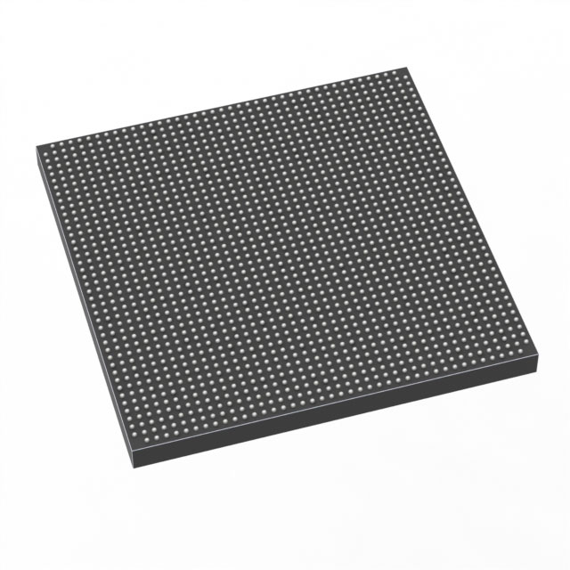
The 1SG280HN3F43E1VGS3 is an Intel Stratix® 10 GX Field Programmable Gate Array delivered in a 1760-BBGA (1760-FBGA, 42.5 × 42.5 mm) package. Designed for high-performance, high-bandwidth applications, this device integrates a large logic fabric with extensive on-chip memory and a high I/O count to support demanding digital signal processing, networking, and compute tasks.
Built on the Stratix® 10 family architecture, the device leverages the family’s core innovations—such as the Hyperflex core architecture and advanced transceiver and hard-IP options—to provide performance and integration for data center, communications, and advanced embedded systems that require high throughput and flexible implementable logic.
Key Features
- Core Architecture Part of the Stratix® 10 GX family with Hyperflex core architecture and 14 nm FinFET technology as described for the family.
- Logic Capacity 2,800,000 logic elements for large-scale logic designs and complex programmable implementations.
- On-chip Memory 240,123,904 total RAM bits to support deep buffering, large lookup tables, and memory-intensive algorithms.
- I/O and Transceivers 688 general-purpose I/O pins and family-level support for heterogeneous 3D SiP transceiver tiles with up to 96 full-duplex transceiver channels and transceiver data rates up to 28.3 Gbps (family capability).
- Hard IP and DSP Stratix® 10 family includes hard PCI Express Gen3 x16 IP, 10G/40G Ethernet FEC in transceivers, and variable-precision DSP blocks capability (family-level features).
- Package & Mounting 1760-BBGA (FCBGA) in a 1760-FBGA supplier package; surface-mount device optimized for board-level integration.
- Power Supply Core voltage supply range: 770 mV to 970 mV, supporting low-voltage core operation.
- Temperature Grade Extended grade operation from 0 °C to 100 °C for applications requiring an extended commercial temperature range.
- Compliance RoHS compliant.
Typical Applications
- High-Speed Networking & Telecom Use the device’s high I/O count, multi-gigabit transceiver capability, and hard Ethernet/forward error-correction IP (family-level) for switches, routers, and line cards.
- Data Center Accelerators Leverage the large logic capacity and abundant on-chip RAM for packet processing, custom acceleration, and preprocessing workloads.
- High-Performance Signal Processing Deploy variable-precision DSP blocks and extensive RAM for wideband signal processing, modulation/demodulation, and software-defined radio functions (family-level features).
- Embedded Compute & SoC Integration Integrate programmable logic with family variants that include embedded processor systems for heterogeneous compute and control tasks.
Unique Advantages
- Large programmable fabric: 2.8 million logic elements provide the capacity to implement complex, large-scale datapaths and control logic on a single device.
- High on-chip memory: 240,123,904 total RAM bits reduce external memory dependence and support deep buffering and large associative structures.
- Extensive I/O and package options: 688 I/O pins combined with a 1760-BBGA package allow dense board-level integration and routing flexibility.
- Family-level transceiver and IP capability: The Stratix® 10 family delivers high-speed transceiver support and hard-IP building blocks—enabling designs that require multi-gigabit links and standardized interfaces (family-level).
- Optimized power envelope: Core supply range of 770 mV–970 mV supports efficient core operation and power planning at board level.
- Extended temperature operation: Rated 0 °C to 100 °C for deployments requiring extended commercial temperature range support.
Why Choose 1SG280HN3F43E1VGS3?
The 1SG280HN3F43E1VGS3 combines a very large logic capacity with significant on-chip RAM and a high I/O count in a compact 1760-BBGA package, positioning it for high-bandwidth, compute-intensive applications. Its voltage and temperature specifications, together with Stratix® 10 family architecture characteristics, make it suitable for designs that need scalable programmable logic, substantial local memory, and robust board-level integration.
This device is well suited to engineering teams building advanced networking, accelerator, and signal processing systems who need a high-capacity FPGA platform backed by the Stratix® 10 family feature set and ecosystem.
Request a quote or submit an inquiry to get pricing, availability, and support details for the 1SG280HN3F43E1VGS3. Our team can help with lead times and volume requirements.





















Date Founded: 1968
Headquarters: Santa Clara, California, USA
Employees: 130,000+
Revenue: $54.23 Billion
Certifications and Memberships: ISO9001:2015, ISO14001:2015, ISO17025:2017, ISO27001:2022, ISO45001:2018, ISO50001:2018


