
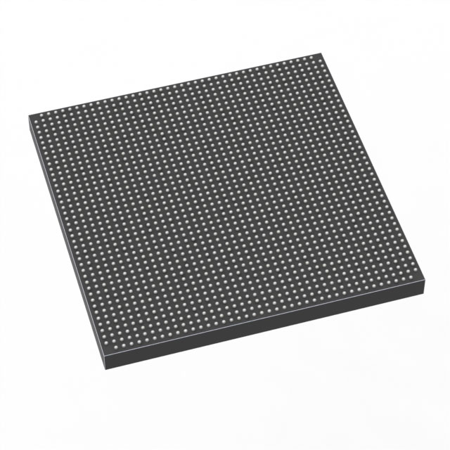
1SG280HU1F50E2VGAS
| Part Description |
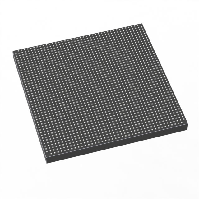
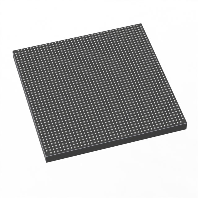
Stratix® 10 GX Field Programmable Gate Array (FPGA) IC 704 2800000 2397-BBGA, FCBGA |
|---|---|
| Quantity | 734 Available (as of October 7, 2026) |
| Product Category | Field Programmable Gate Array (FPGA) |
|---|---|
| Manufacturer | Intel |
| Manufacturing Status | Active |
| Manufacturer Standard Lead Time | 12 Weeks |
| Datasheet |
Specifications & Environmental
| Device Package | 2397-FBGA, FC (50x50) | Grade | Extended | Operating Temperature | 0°C – 100°C | ||
|---|---|---|---|---|---|---|---|
| Package / Case | 2397-BBGA, FCBGA | Number of I/O | 704 | Voltage | 770 mV - 970 mV | ||
| Mounting Method | Surface Mount | RoHS Compliance | Unknown | REACH Compliance | REACH Unaffected | ||
| Moisture Sensitivity Level | 3 (168 Hours) | Number of LABs/CLBs | 350000 | Number of Logic Elements/Cells | 2800000 | ||
| Number of Gates | N/A | ECCN | N/A | HTS Code | N/A | ||
| Qualification | N/A | Total RAM Bits | 240123904 |
Overview of 1SG280HU1F50E2VGAS – Stratix® 10 GX Field Programmable Gate Array (FPGA)
The 1SG280HU1F50E2VGAS is an Intel Stratix® 10 GX FPGA in a 2397-BBGA (FCBGA) package designed for high-density, high-bandwidth system designs. It integrates the Stratix 10 family innovations, including the Intel Hyperflex™ core architecture and heterogeneous transceiver technology, and targets applications that require large programmable fabric, substantial on-chip RAM, and extensive I/O resources.
With 2,800,000 logic elements and 240,123,904 bits of on-chip RAM, this device is tailored for advanced communications, data-center, and compute-accelerator roles where throughput, integration, and flexible I/O are primary concerns.
Key Features
- Core Architecture Built on the Intel Stratix 10 family with the Intel Hyperflex™ core architecture, delivering increased core performance compared to previous-generation high-performance FPGAs as described in the Stratix 10 device overview.
- Logic Density Approximately 2,800,000 logic elements, enabling very large-scale programmable designs and complex logic implementations.
- On‑Chip Memory 240,123,904 total RAM bits to support large buffering, caching, and shared memory use cases within the FPGA fabric.
- I/O and Connectivity 704 I/O pins provide broad external interface capability; Stratix 10 family transceiver technology (described in the device overview) supports high-speed serial links and advanced protocol IP.
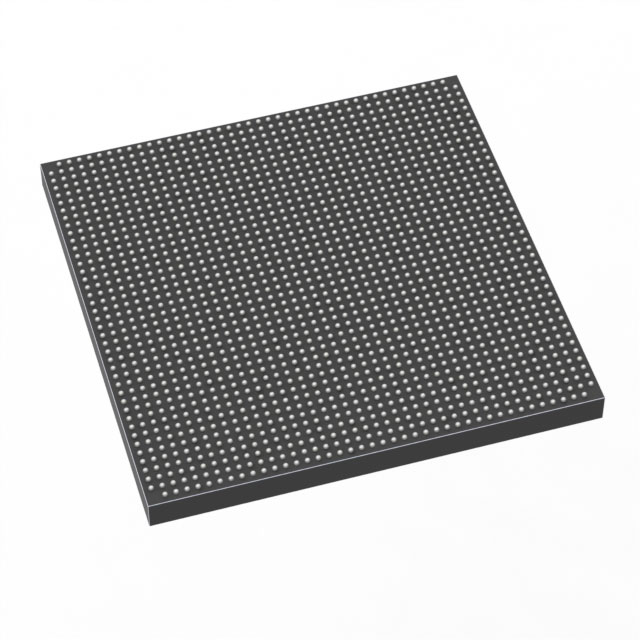
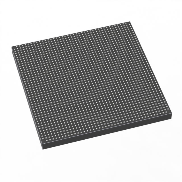
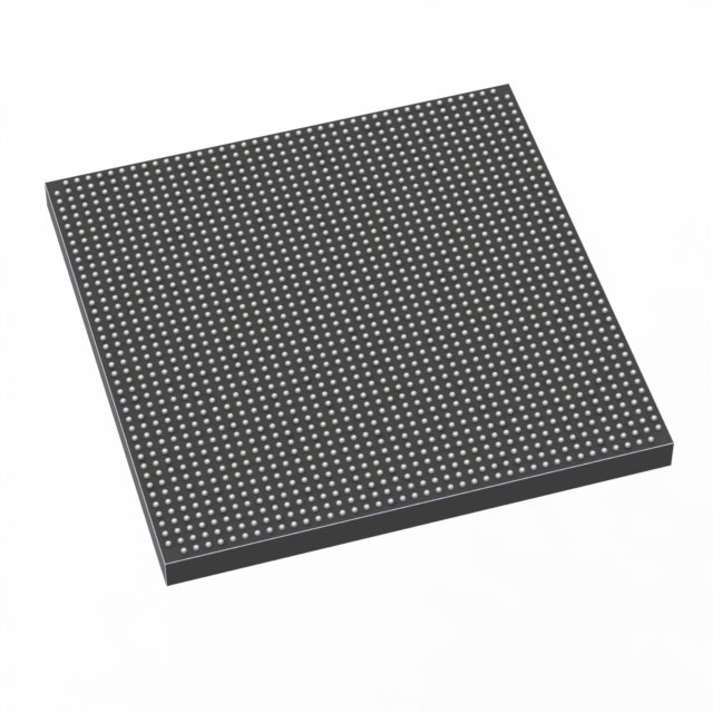
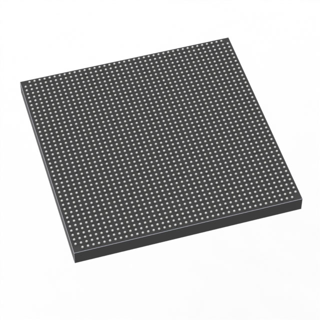
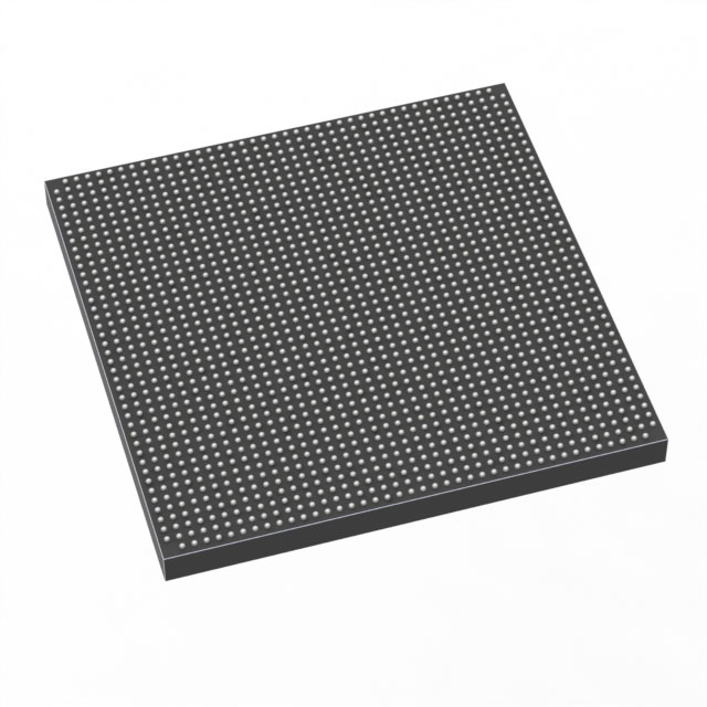
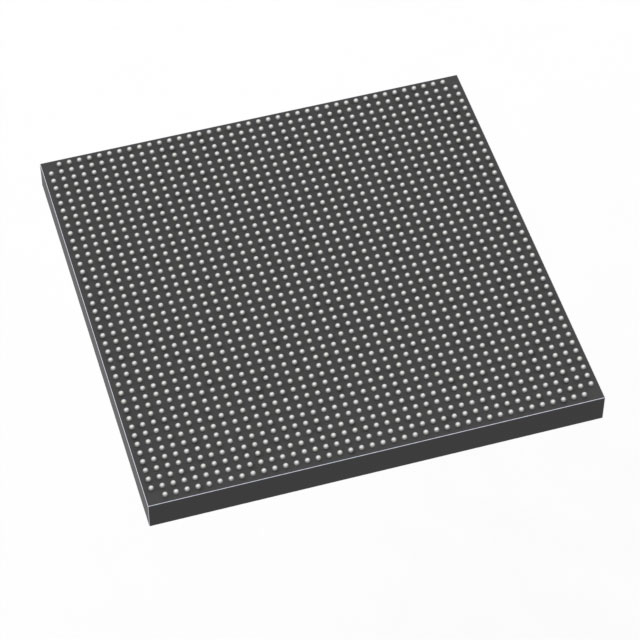
- Package and Mounting 2397-BBGA (FCBGA) supplier device package (2397-FBGA, FC 50×50) with surface-mount mounting type for compact board implementations.
- Power and Supply Core voltage supply range specified at 770 mV to 970 mV to match high-performance Stratix 10 power domains.
- Operating Range Extended grade with an operating temperature range of 0 °C to 100 °C suitable for elevated-temperature applications that fall within this range.
- Family-Level IP and Features Stratix 10 family documentation highlights hard IP options such as PCI Express Gen3, high-speed Ethernet and FEC, DDR4 memory controllers, and variable-precision DSP blocks—capabilities available within the Stratix 10 device family.
- Regulatory RoHS compliant.
Typical Applications
- High‑speed networking and switching Use the device where high-bandwidth serial links and hard 10G/40G Ethernet IP (as provided by the Stratix 10 family) are required for backplane and module connectivity.
- Data‑center acceleration Leverage the large logic element count and on‑chip RAM for custom packet processing, protocol offload, or hardware-accelerated compute tasks.
- Telecommunications infrastructure Deploy in systems needing dense programmable fabric and advanced transceiver capabilities for line cards, aggregation, or transport equipment.
- High‑performance DSP and signal processing Implement intensive DSP workloads using Stratix 10 family variable-precision DSP resources and extensive on-chip memory.
Unique Advantages
- High programmable density: 2,800,000 logic elements enable large, complex designs without immediate need for multiple devices.
- Substantial on‑chip memory: 240,123,904 bits of RAM reduce dependence on external memory for many buffering and caching tasks.
- Extensive external connectivity: 704 I/O pins provide flexible interfacing options for dense system integration.
- Family-level advanced IP: Access to Stratix 10 GX/SX family features such as high-speed transceivers, PCIe, and DSP blocks simplifies implementation of common high-performance subsystems.
- Robust packaging for dense boards: 2397-BBGA (FCBGA) in a surface-mount format supports compact, high‑component‑density PCB designs.
- Controlled power domain: Core supply specified between 770 mV and 970 mV allows predictable power planning for high-performance cores.
Why Choose 1SG280HU1F50E2VGAS?
The 1SG280HU1F50E2VGAS delivers the capabilities of the Stratix 10 GX family in a high-density FCBGA package, combining multi-million logic-element capacity with large on-chip RAM and broad I/O. It is positioned for engineers building high-throughput, compute- and bandwidth‑intensive systems that benefit from Stratix 10 family architectures and device‑level features.
For designs that require scalable programmable fabric, substantial embedded memory, and advanced I/O/transceiver resources within an extended operating-temperature range, this device offers a concrete platform that aligns with the Stratix 10 GX device overview and specifications provided in the product documentation.
Request a quote or submit an inquiry to get pricing and availability for the 1SG280HU1F50E2VGAS and discuss how it fits your next high-performance FPGA design.





















Date Founded: 1968
Headquarters: Santa Clara, California, USA
Employees: 130,000+
Revenue: $54.23 Billion
Certifications and Memberships: ISO9001:2015, ISO14001:2015, ISO17025:2017, ISO27001:2022, ISO45001:2018, ISO50001:2018


