
1SG280HU3F50E1VG
| Part Description |
Stratix® 10 GX Field Programmable Gate Array (FPGA) IC 704 2800000 2397-BBGA, FCBGA |
|---|---|
| Quantity | 726 Available (as of June 15, 2026) |

| Product Category | Field Programmable Gate Array (FPGA) |
|---|---|
| Manufacturer | Intel |
| Manufacturing Status | Active |
| Manufacturer Standard Lead Time | 12 Weeks |
| Datasheet |
Specifications & Environmental
| Device Package | 2397-FBGA, FC (50x50) | Grade | Extended | Operating Temperature | 0°C – 100°C | ||
|---|---|---|---|---|---|---|---|
| Package / Case | 2397-BBGA, FCBGA | Number of I/O | 704 | Voltage | 770 mV - 970 mV | ||
| Mounting Method | Surface Mount | RoHS Compliance | Unknown | REACH Compliance | REACH Unaffected | ||
| Moisture Sensitivity Level | 3 (168 Hours) | Number of LABs/CLBs | 350000 | Number of Logic Elements/Cells | 2800000 | ||
| Number of Gates | N/A | ECCN | N/A | HTS Code | N/A | ||
| Qualification | N/A | Total RAM Bits | 240123904 |
Overview of 1SG280HU3F50E1VG – Stratix® 10 GX FPGA, 2,800,000 logic elements, 704 I/O
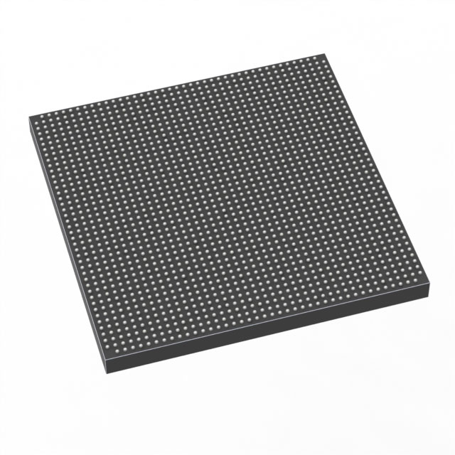
The 1SG280HU3F50E1VG is an Intel Stratix 10 GX field programmable gate array (FPGA) in a 2397-BBGA FCBGA package. It combines the Stratix 10 family’s Hyperflex core architecture and 14 nm tri-gate (FinFET) technology with high logic density and extensive I/O for advanced, high-bandwidth applications.
Targeted at designs that require large programmable fabric, substantial on-chip memory and high-speed connectivity, this device delivers 2,800,000 logic elements, roughly 240,123,904 bits of embedded RAM, and 704 user I/O. The part is offered in an Extended grade with a 0 °C to 100 °C operating range and RoHS compliance.
Key Features
- Core Architecture Built on the Intel Stratix 10 GX family with the Hyperflex core architecture and Intel 14 nm tri-gate (FinFET) technology to support demanding logic and timing requirements.
- Logic Capacity 2,800,000 logic elements providing large programmable fabric for complex designs and high gate counts.
- On‑Chip Memory Approximately 240,123,904 total RAM bits of embedded memory for buffering, large tables, and intermediate storage without external DRAM.
- I/O and Transceivers 704 user I/O pins combined with Stratix 10 family transceiver capabilities; the series supports heterogeneous 3D SiP transceiver tiles with up to 96 full‑duplex channels and transceiver data rates up to 28.3 Gbps (series-level).
- Interfaces and Hard IP (series-level) Stratix 10 series documentation includes hard IP options such as PCI Express Gen3, 10G Ethernet, and Interlaken to accelerate interface implementation.
- Power Supply Core voltage range specified from 770 mV to 970 mV, enabling compatibility with Stratix 10 family power management approaches.
- Package & Mounting 2397-BBGA (FCBGA) surface-mount package; supplier device package noted as 2397-FBGA, FC (50×50).
- Grade & Temperature Extended grade device with an operating temperature range of 0 °C to 100 °C.
- Regulatory RoHS compliant.
Typical Applications
- High‑speed Networking and Telecom Use the device’s large logic fabric, on‑chip memory, and high‑speed transceivers to implement packet processing, switch fabric, and forward error correction functions.
- Data Center Acceleration Deploy as an accelerator for compute offload, custom protocol handling and PCIe‑connected modules using Stratix 10 family interface IP.
- Signal Processing and RF Leverage the abundant logic elements and embedded RAM for real‑time DSP pipelines, filtering, and buffering in communications and radar systems.
- Backplane and Module Interconnects High transceiver performance and numerous I/O make the device suitable for high‑bandwidth backplane and board‑to‑board interfaces.
Unique Advantages
- High Logic Density: 2,800,000 logic elements enable larger, more complex designs without partitioning across multiple devices.
- Substantial On‑Chip Memory: ~240 million RAM bits reduce reliance on external memory for many buffering and state‑storage use cases.
- Extensive I/O and High‑Speed Links: 704 I/O pins and Stratix 10 series transceivers support high port counts and multi‑gigabit connectivity.
- Modern Process Technology: Intel 14 nm tri‑gate (FinFET) and Hyperflex architecture provide the series-level performance and timing characteristics designers expect from Stratix 10 devices.
- Compact, Surface‑Mount Package: 2397‑BBGA FCBGA package in a 50×50 supplier format supports dense board integration and module designs.
- Extended Operating Range: Rated for 0 °C to 100 °C and RoHS compliant for broad deployment scenarios.
Why Choose 1SG280HU3F50E1VG?
The 1SG280HU3F50E1VG positions itself for projects that demand very large programmable capacity, substantial embedded memory and extensive high‑speed I/O in a single Stratix 10 GX device. Its combination of 2.8 million logic elements, large RAM resource, and series‑level transceiver and interface capabilities make it suitable for advanced networking, compute acceleration and high‑performance signal processing designs.
As part of the Intel Stratix 10 family, the device benefits from Stratix 10 architecture and supporting documentation, helping development teams scale designs within the same device family and leverage available hard IP and transceiver resources.
Request a quote or submit an inquiry to receive pricing, availability and lead‑time information for the 1SG280HU3F50E1VG.


Date Founded: 1968
Headquarters: Santa Clara, California, USA
Employees: 130,000+
Revenue: $54.23 Billion
Certifications and Memberships: ISO9001:2015, ISO14001:2015, ISO17025:2017, ISO27001:2022, ISO45001:2018, ISO50001:2018


