
1SG280HU3F50E2VG
| Part Description |
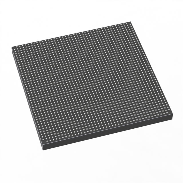
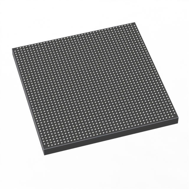
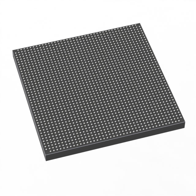
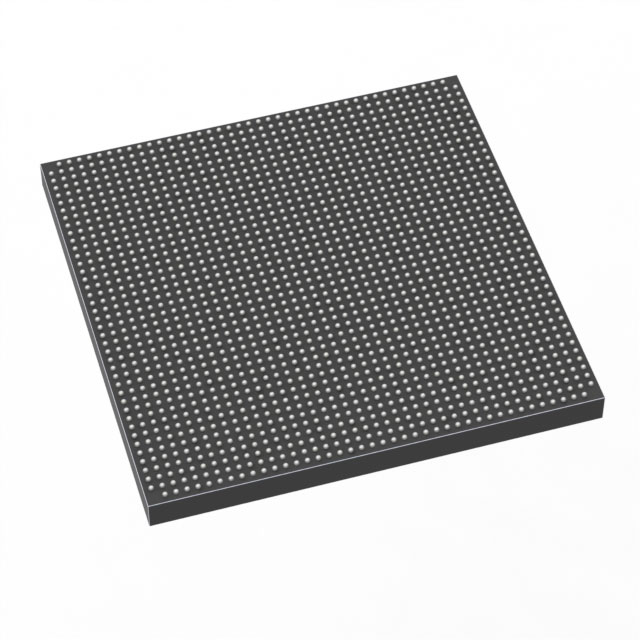
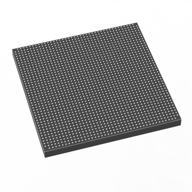
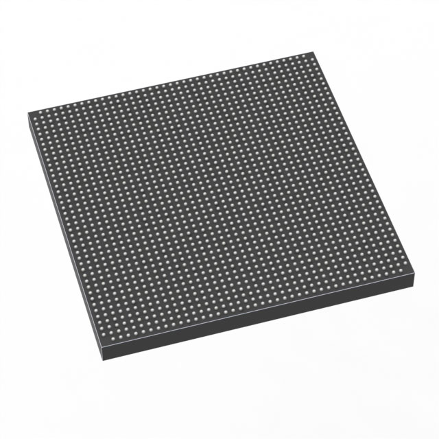
Stratix® 10 GX Field Programmable Gate Array (FPGA) IC 704 2800000 2397-BBGA, FCBGA |
|---|---|
| Quantity | 27 Available (as of October 8, 2026) |
| Product Category | Field Programmable Gate Array (FPGA) |
|---|---|
| Manufacturer | Intel |
| Manufacturing Status | Active |
| Manufacturer Standard Lead Time | 12 Weeks |
| Datasheet |
Specifications & Environmental
| Device Package | 2397-FBGA, FC (50x50) | Grade | Extended | Operating Temperature | 0°C – 100°C | ||
|---|---|---|---|---|---|---|---|
| Package / Case | 2397-BBGA, FCBGA | Number of I/O | 704 | Voltage | 770 mV - 970 mV | ||
| Mounting Method | Surface Mount | RoHS Compliance | Unknown | REACH Compliance | REACH Unaffected | ||
| Moisture Sensitivity Level | 3 (168 Hours) | Number of LABs/CLBs | 350000 | Number of Logic Elements/Cells | 2800000 | ||
| Number of Gates | N/A | ECCN | N/A | HTS Code | N/A | ||
| Qualification | N/A | Total RAM Bits | 240123904 |
Overview of 1SG280HU3F50E2VG – Stratix® 10 GX FPGA, 2,800,000 logic elements, 704 I/Os, 2397‑BBGA
The 1SG280HU3F50E2VG is an Intel Stratix® 10 GX field programmable gate array (FPGA) in a 2397‑ball FCBGA package designed for high‑density, performance‑focused system designs. The device combines a large logic fabric with substantial on‑chip memory and a high I/O count to address advanced applications that require significant programmable logic, bandwidth and system integration.
Built around the Stratix 10 GX family architecture, this device targets demanding compute and signal‑processing roles where core performance, a large RAM budget and flexible I/O are primary design drivers.
Key Features
- Core Architecture Approximately 2,800,000 logic elements deliver the programmable fabric capacity needed for large, complex designs.
- On‑Chip Memory 240,123,904 total RAM bits provide substantial embedded SRAM for buffering, frame storage and local working memory.
- I/O Density 704 device I/Os support extensive external connectivity and multiple parallel interfaces.
- Package & Mounting 2397‑BBGA FCBGA package (supplier package: 2397‑FBGA, FC 50×50) in a surface‑mount format supports high pin count board implementations.
- Power Supply Core voltage support in the range 770 mV to 970 mV enables integration with modern low‑voltage power architectures.
- Operating Conditions Extended grade device rated for operation from 0 °C to 100 °C, suitable for applications requiring that temperature range.
- Family‑Level Innovations Based on the Stratix 10 GX family architecture, which includes Intel Hyperflex core techniques and Intel 14 nm tri‑gate process innovations (series‑level features documented in the Stratix 10 GX overview).
Typical Applications
- High‑bandwidth networking and switching Large logic capacity and high I/O count enable packet processing, forwarding engines and protocol implementation where on‑chip resources and I/O density matter.
- Compute acceleration and hardware offload The combination of dense logic and extensive embedded RAM supports FPGA‑based acceleration for algorithmic workloads and custom datapaths.
- Signal processing and DSP Substantial on‑chip memory and logic resources suit real‑time filtering, encoding/decoding and other high‑throughput signal processing tasks.
- Prototyping and system integration High pin‑count package and surface‑mount form factor enable integration into complex boards for prototype and production systems requiring significant programmable resources.
Unique Advantages
- High logic density: 2,800,000 logic elements provide headroom for large, multi‑function designs without partitioning across multiple devices.
- Large embedded RAM: 240,123,904 total RAM bits reduce reliance on external memory for buffering and intermediate storage, simplifying board design and improving latency.
- Extensive I/O: 704 device I/Os support parallel interfaces and high‑pin‑count connectivity for complex peripheral and subsystem integration.
- Compact, manufacturable package: 2397‑ball FCBGA surface‑mount package supports dense board layouts while providing the pin count required for high‑performance systems.
- Low‑voltage core operation: 770 mV–970 mV supply range aligns with contemporary low‑power supply rails common in advanced system designs.
- Extended operating range: 0 °C to 100 °C rating fits applications with moderate thermal requirements where extended‑grade components are specified.
Why Choose 1SG280HU3F50E2VG?
1SG280HU3F50E2VG positions itself as a high‑capacity Stratix 10 GX FPGA option for designs that need substantial programmable logic, large on‑chip memory and a large I/O portfolio in a single‑chip solution. Its device‑level specs make it suitable for system architects who require dense logic fabrics and significant RAM on the device to minimize external memory dependency and simplify system partitioning.
For teams building advanced networking, compute acceleration, or high‑throughput signal processing products, this device delivers the programmable resources, package density and operating characteristics required to scale complex designs while leveraging the Stratix 10 GX family architecture.
Request a quote or submit an inquiry to check pricing and availability for 1SG280HU3F50E2VG and to discuss how this Stratix® 10 GX FPGA can fit into your next design.





















Date Founded: 1968
Headquarters: Santa Clara, California, USA
Employees: 130,000+
Revenue: $54.23 Billion
Certifications and Memberships: ISO9001:2015, ISO14001:2015, ISO17025:2017, ISO27001:2022, ISO45001:2018, ISO50001:2018


