
1SG280HU3F50E3VG
| Part Description |
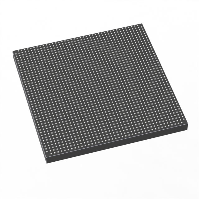
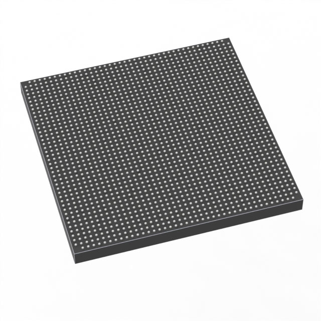
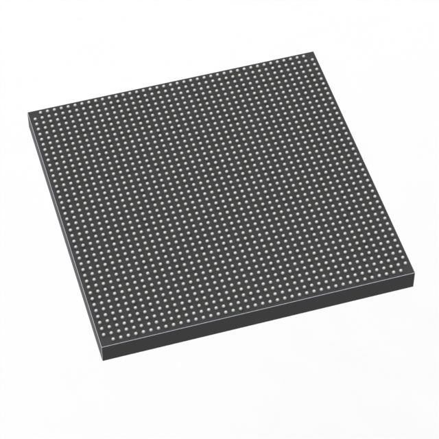
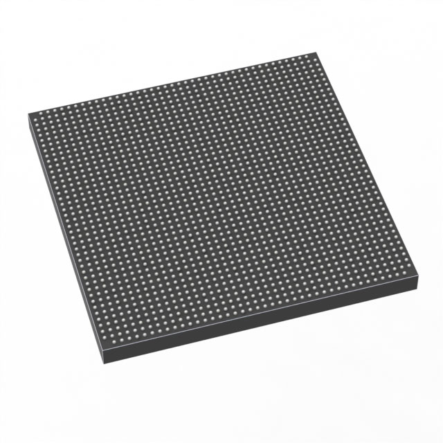
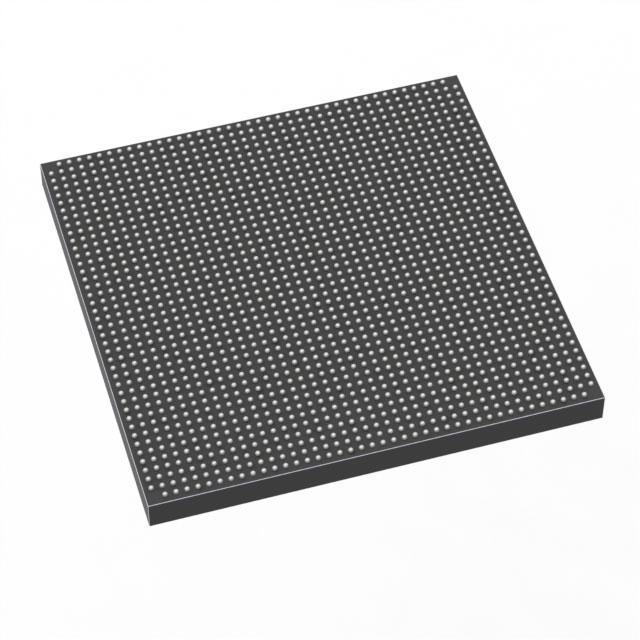
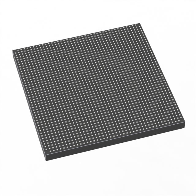
Stratix® 10 GX Field Programmable Gate Array (FPGA) IC 704 2800000 2397-BBGA, FCBGA |
|---|---|
| Quantity | 190 Available (as of October 8, 2026) |
| Product Category | Field Programmable Gate Array (FPGA) |
|---|---|
| Manufacturer | Intel |
| Manufacturing Status | Active |
| Manufacturer Standard Lead Time | 12 Weeks |
| Datasheet |
Specifications & Environmental
| Device Package | 2397-FBGA, FC (50x50) | Grade | Extended | Operating Temperature | 0°C – 100°C | ||
|---|---|---|---|---|---|---|---|
| Package / Case | 2397-BBGA, FCBGA | Number of I/O | 704 | Voltage | 770 mV - 970 mV | ||
| Mounting Method | Surface Mount | RoHS Compliance | Unknown | REACH Compliance | REACH Unaffected | ||
| Moisture Sensitivity Level | 3 (168 Hours) | Number of LABs/CLBs | 350000 | Number of Logic Elements/Cells | 2800000 | ||
| Number of Gates | N/A | ECCN | N/A | HTS Code | N/A | ||
| Qualification | N/A | Total RAM Bits | 240123904 |
Overview of 1SG280HU3F50E3VG – Stratix® 10 GX FPGA, 2,800,000 logic elements, 704 I/O
The 1SG280HU3F50E3VG is a high-density Stratix® 10 GX Field Programmable Gate Array (FPGA) offered in a 2397-BBGA FCBGA package. It delivers large on-chip logic and memory resources together with extensive I/O for demanding bandwidth and compute applications.
As part of the Stratix 10 GX family, this device benefits from family-level innovations such as the Intel Hyperflex™ core architecture and Intel 14 nm tri-gate (FinFET) process, which target increased core performance and improved power efficiency for data center, networking and high-performance compute applications.
Key Features
- Core Architecture (family-level) Family innovations include the Intel Hyperflex™ core architecture and Intel 14 nm tri-gate (FinFET) technology, designed to increase core performance and reduce power compared to previous-generation high-performance FPGAs.
- Logic Capacity 2,800,000 logic elements to implement large, complex designs and high-density custom logic.
- On-chip Memory 240,123,904 total RAM bits for buffering, data staging and embedded storage requirements.
- I/O and Transceivers 704 user I/O pins to interface with high-speed peripherals and wide external buses. Family-level transceiver technology supports multi-gigabit serial links and advanced PHY features.
- Hard IP (family-level) Stratix 10 GX family documentation details available hard IP such as PCI Express Gen1/Gen2/Gen3 and industry-standard protocol blocks to accelerate system integration.
- Power and Voltage Core supply range 770 mV to 970 mV to match system power architectures and optimize performance/power trade-offs.
- Package and Mounting 2397-BBGA FCBGA (2397-FBGA, FC 50×50) surface-mount package for high-pin-count board layouts.
- Operating Range and Grade Extended grade with an operating temperature range of 0°C to 100°C and RoHS compliance for regulatory alignment.
Typical Applications
- Network and Telecom Platforms High logic density and extensive I/O support packet processing, protocol offload and multi-gigabit connectivity in switches, routers and line cards.
- Data Center Acceleration Large on-chip RAM and abundant logic elements enable custom acceleration engines for compute and storage workloads.
- High-Performance Test & Measurement Wide I/O count and family-level transceiver capabilities suit high-channel-count acquisition and timing-sensitive instrumentation.
- Communication Infrastructure Hard IP blocks and high-speed serial capabilities support implementation of communication protocols and interface bridging.
Unique Advantages
- High logic density: 2.8 million logic elements provide the capacity to implement complex algorithms and large-scale digital designs on a single device.
- Large embedded memory: 240,123,904 total RAM bits reduce dependence on external memory for many buffering and data-path needs.
- Extensive I/O: 704 I/O pins enable broad interfacing options for parallel buses, high-pin-count peripherals and board-level routing flexibility.
- Family-level performance innovations: The Stratix 10 GX family leverages Hyperflex architecture and 14 nm FinFET technology to improve core performance and power efficiency versus previous generations.
- System integration options: Documented family hard IP (PCIe, Ethernet, protocol blocks) helps accelerate system design and reduce integration time.
- Production-ready packaging and compliance: 2397-BBGA FCBGA surface-mount package and RoHS compliance support high-density production boards and regulatory requirements.
Why Choose 1SG280HU3F50E3VG?
The 1SG280HU3F50E3VG positions itself for designs that require very high logic capacity, substantial on-chip memory and a large number of I/Os in a single FPGA package. It is suitable for system designers building networking, data center acceleration, communications and high-performance measurement equipment where integrating large custom logic and fast interfaces is essential.
As a member of the Stratix 10 GX family, this device benefits from family-level architectural advances and documented hard IP that help shorten development cycles and provide a scalable path for future design iterations.
Request a quote or submit an inquiry for pricing, availability and lead time for the 1SG280HU3F50E3VG.





















Date Founded: 1968
Headquarters: Santa Clara, California, USA
Employees: 130,000+
Revenue: $54.23 Billion
Certifications and Memberships: ISO9001:2015, ISO14001:2015, ISO17025:2017, ISO27001:2022, ISO45001:2018, ISO50001:2018


