
1SG280HU3F50I1VG
| Part Description |
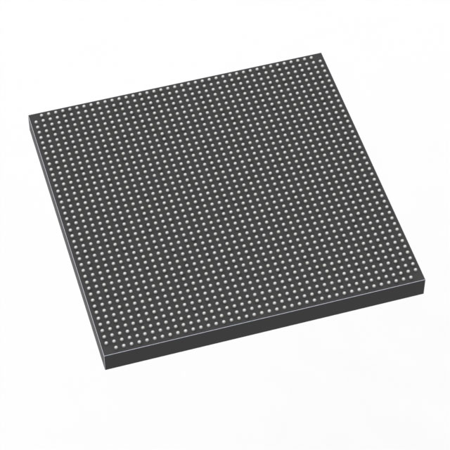
Stratix® 10 GX Field Programmable Gate Array (FPGA) IC 704 2800000 2397-BBGA, FCBGA |
|---|---|
| Quantity | 1,487 Available (as of June 15, 2026) |

| Product Category | Field Programmable Gate Array (FPGA) |
|---|---|
| Manufacturer | Intel |
| Manufacturing Status | Active |
| Manufacturer Standard Lead Time | 12 Weeks |
| Datasheet |
Specifications & Environmental
| Device Package | 2397-FBGA, FC (50x50) | Grade | Industrial | Operating Temperature | -40°C – 100°C | ||
|---|---|---|---|---|---|---|---|
| Package / Case | 2397-BBGA, FCBGA | Number of I/O | 704 | Voltage | 770 mV - 970 mV | ||
| Mounting Method | Surface Mount | RoHS Compliance | Unknown | REACH Compliance | REACH Unaffected | ||
| Moisture Sensitivity Level | 3 (168 Hours) | Number of LABs/CLBs | 350000 | Number of Logic Elements/Cells | 2800000 | ||
| Number of Gates | N/A | ECCN | N/A | HTS Code | N/A | ||
| Qualification | N/A | Total RAM Bits | 240123904 |
Overview of 1SG280HU3F50I1VG – Stratix® 10 GX Field Programmable Gate Array (FPGA) IC, 704 I/O, 2397-BBGA
The 1SG280HU3F50I1VG is an Intel Stratix® 10 GX family FPGA in a 2397-BBGA (FCBGA) package, featuring a high logic capacity and extensive on-chip memory. It implements Intel’s Hyperflex core architecture and 14 nm FinFET innovations at the family level, targeting high-bandwidth, high-performance digital designs.
With 2,800,000 logic elements, 240,123,904 bits of on-chip RAM and 704 I/O, this device is suited for demanding applications that require dense logic, large embedded memory and a wide range of I/O connectivity, all in an industrial-grade, surface-mount package.
Key Features
- Core Architecture Family-level Intel Hyperflex core architecture and 14 nm tri-gate (FinFET) technology are described in the device overview for Stratix® 10 GX, delivering the class-level performance and efficiency innovations of the family.
- Logic Capacity 2,800,000 logic elements provide extensive programmable logic resources for complex algorithms, packet processing and high-density control functions.
- Embedded Memory 240,123,904 total on-chip RAM bits enable large buffering, lookup tables and memory-intensive compute tasks without immediate dependence on external DRAM.
- I/O 704 device I/O pins support broad interface options and high pin-count system integration.
- Package & Mounting 2397-BBGA, FCBGA package (supplier package: 2397-FBGA, FC, 50×50) in a surface-mount form factor for compact board-level integration.
- Power Supported core voltage range from 770 mV to 970 mV to match system power-rail planning and regulator selection.
- Temperature & Grade Industrial grade operation from -40°C to 100°C for deployment in temperature-challenging environments.
- Standards & Compliance RoHS compliant for adherence to common environmental requirements.
Typical Applications
- High‑performance networking and switching Large logic and memory resources with high I/O count support packet processing, complex protocol engines and high-throughput data paths.
- Telecommunications infrastructure Dense programmable logic and extensive embedded RAM enable implementation of line-rate functions, forward error correction and protocol IP blocks described at the device family level.
- Signal processing and acceleration High logic element count and on-chip RAM support DSP pipelines, fixed/floating point datapaths and custom acceleration kernels.
- Embedded compute platforms The Stratix® 10 family overview includes SoC variants and hard-IP features; this device’s logic, memory and I/O density make it suitable for complex FPGA-centric systems.
Unique Advantages
- Very high programmable capacity: 2,800,000 logic elements enable integration of large, system-level functions on a single device, reducing external logic count.
- Large on-chip RAM: 240,123,904 bits of embedded RAM minimize external memory dependence for buffering and lookup operations.
- Extensive I/O footprint: 704 I/Os provide flexibility to connect multiple high-pin-count interfaces directly to the FPGA.
- Industrial temperature range: Rated for -40°C to 100°C, supporting deployments in industrial environments.
- High-density FCBGA package: 2397-BBGA (2397-FBGA, FC 50×50) simplifies high-pin-count board routing in a compact surface-mount form factor.
- Family-level performance and innovation: Built on the Stratix® 10 GX family foundation (Hyperflex architecture, 14 nm FinFET, and advanced transceiver and IP options described in the device overview), enabling designs that leverage those class-level capabilities.
Why Choose 1SG280HU3F50I1VG?
The 1SG280HU3F50I1VG provides a combination of very high logic density, substantial on-chip RAM and a large I/O count in an industrial-grade FCBGA package. It is positioned for engineers building high-throughput networking, telecommunications, DSP acceleration and embedded compute platforms that require dense programmable resources and robust thermal operation.
Backed by the Stratix® 10 GX family architecture and Intel’s documented device features, this FPGA offers designers scalability and integration potential for complex system designs while maintaining RoHS compliance and industrial temperature capability.
Request a quote or submit a purchasing inquiry to evaluate 1SG280HU3F50I1VG for your next high-performance FPGA design.


Date Founded: 1968
Headquarters: Santa Clara, California, USA
Employees: 130,000+
Revenue: $54.23 Billion
Certifications and Memberships: ISO9001:2015, ISO14001:2015, ISO17025:2017, ISO27001:2022, ISO45001:2018, ISO50001:2018


